Cladding-Free Photonic Circuits Boost Dense On-Chip Integration
The integration of photonic circuits in a single, chip-scale device is crucial for future high-speed, light-based information processing and communication. Realizing these applications requires further miniaturization of photonic waveguides, but all photonic waveguides designed so far require cladding layers that physically separate adjacent channels from each other. This has imposed a fundamental limit on the miniaturization of photonic circuits. Now, Yun Lai from Nanjing University, China, and his colleagues report an ingenious demonstration of a waveguiding mechanism that eliminates the need for cladding layers in photonic circuits [1]. These findings not only extend the current understanding of waveguiding physics, but they also provide an opportunity to construct ultracompact photonic circuits that can overcome the miniaturization limit by providing 100% utilization of the on-chip space.
In order for light to be guided so that it propagates in a specific direction—for example, in a communications network—the light needs to be confined in an information channel such as an optical fiber. Such optical confinement in low-loss dielectric materials can be realized generally through two mechanisms, both of which rely on cladding layers. The first is total internal reflection [2]. When a ray of light strikes an interface that separates one medium from another, the ray can be fully reflected if the second medium has a lower refractive index and the incident angle of the incoming wave exceeds the critical angle. In this case, the second medium serves as the cladding layer that forbids wave propagation. The other mechanism for optical confinement is through a photonic crystal with a band gap [3]. The band gap is a frequency range where wave propagation is fully forbidden in all directions. Therefore, a gapped photonic crystal can serve as the cladding layer to guide light via an empty region embedded in the crystal [3].
These wave-forbidden cladding layers are not only necessary for guiding light along straight channels, but they are also critical in constructing bends for routing waves around curves. A bend in wave propagation means a large change in momentum, which can cause significant scattering. In waveguides based on total internal reflection, a bend typically requires a large radius comprising tens of wavelengths. In contrast, a sharp bend with zero radius is possible in a photonic-crystal band-gap waveguide with a specifically optimized bend shape [4]. Either way, wave propagation around a bend requires wave-forbidden cladding layers.
The existence of a minimum thickness for cladding layers imposes a fundamental limit on the miniaturization of photonic integration. Many efforts have been made to squeeze the cladding layers into a smaller space [5, 6], but none have managed to fully remove them. In this study, Lai and colleagues have taken several steps to achieve this ultimate goal.
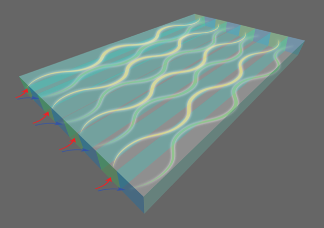
The team first designed a special dielectric cladding material, which is a photonic crystal whose spatial dispersion, or isofrequency contour, is no longer centered in momentum space. Rather, because the two materials have different dispersion properties, contours for the same light frequencies are offset from each other in momentum space. Amazingly, using such a material in the cladding layers in a waveguide array allowed both the cladding layers and the original waveguide channels to guide light (Fig. 1). Each layer in the waveguide functioned simultaneously as an information channel and an effective cladding layer that separated neighboring channels. In other words, cladding layers became informational channels too. This waveguiding mechanism differs from photonic-crystal band-gap waveguiding because no band gap is involved. It also differs from the total internal reflection in conventional fibers because, here, the total internal reflection works from both sides of an interface. The spatial dispersions of neighboring layers have no overlap, allowing any incident wave to be fully reflected.
The team then designed the surface impedance of the dispersion-shifted material to match that of free space (or air) at the input and output of the waveguide channels. This impedance matching guarantees negligible reflection of the transmitted light between the material and air on a surface perpendicular to the waveguiding direction—including the square-shaped regions of air at the points where two straight waveguides meet. As a consequence, by properly arranging building blocks of the dispersion-shifted material and air, the team was able to demonstrate zero-radius sharp bending of waveguides with negligible leakage of light to the environment through these corner regions of air. Most impressively, the team demonstrated wave routing that traverses the entire physical space through zigzag paths—like a “maze” for photons without physical “walls” (i.e., cladding layers). The team had previously demonstrated similar ultratransparency using a dispersion-shifted photonic crystal in the field of transformation optics [7, 8]. Here, they show for the first time that the concept applies to waveguiding physics, where it promises to shift the waveguiding paradigm.
A few limitations of this technique still need to be addressed. First, Lai and colleagues performed their demonstration at microwave frequencies. Although Maxwell’s equations describe both microwave and optical regimes, a question still remains as to whether phenomena including the maze-like wave routing can be realized at optical frequencies. For example, the fabricated rods may not be ideal rectangles. As a result, the isofrequency contour could change, which could then degrade the performance. Second, the team completed their analysis with two-dimensional geometries. How to extend the theory and design to realistic three-dimensional waveguide systems requires further discussions. Finally, although each photonic crystal layer serves as an effective cladding for its neighboring waveguide layers, the photonic crystal layers and the waveguide layers must be sufficiently wide to avoid evanescent coupling between next-nearest-neighbor channels. Further studies, involving the engineering of multiple layers with different amounts of dispersion shifting, need be conducted along these lines.
Nevertheless, this research has clearly overturned a long-held tenet in waveguiding physics—that wave-forbidden cladding layers are necessary for guided light propagation. By turning cladding layers into waveguides, the speed and capacity of on-chip information delivery could be dramatically increased. Moreover, the possibility of wave routing without cladding layers—like building highways without median strips for light—will allow the on-chip designs in which the entire chip can be utilized for photonic integration, reaching the absolute miniaturization limit. We can also envision that such a universal mechanism could be applied in other wave systems, both classical and quantum, such as surface plasmons and quantum qubit manipulation in optical quantum computers.
References
- T. Song et al., “Ultracompact photonic circuits without cladding layers,” Phys. Rev. X 12, 011053 (2022).
- J. A. Kong, Electromagnetic Wave Theory (EMW Publishing, Cambridge, 2008)[Amazon][WorldCat].
- J. D. Joannopoulos et al., Photonic Crystals: Molding the Flow of Light, 2nd edition (Princeton University Press, Princeton, 2008)[Amazon][WorldCat].
- S. Y. Lin et al., “Experimental demonstration of guiding and bending of electromagnetic waves in a photonic crystal,” Science 282, 274 (1998).
- S. Jahani et al., “Controlling evanescent waves using silicon photonic all-dielectric metamaterials for dense integration,” Nat. Comm. 9, 1893 (2018).
- M. B. Mia et al., “Exceptional coupling in photonic anisotropic metamaterials for extremely low waveguide crosstalk,” Optica 7, 881 (2020).
- J. Luo et al., “Ultratransparent media and transformation optics with shifted spatial dispersions,” Phys. Rev. Lett. 117, 223901 (2016).
- S. Li et al., “Observation of wide-angle impedance matching in terahertz photonic crystals,” New J. Phys. 22, 023033 (2020).