Beaming in a Spin Texture
Spin-based electronic, or “spintronic,” devices can benefit from techniques that coax electron spins into static spatial patterns called spin textures. A new experiment demonstrates that an optical vortex—a light beam that carries orbital angular momentum—can generate a stable spin texture in a semiconductor [1]. The research team showed that the vortex generates a pattern of stripes that has potential uses in processing spin information. Previous experiments have optically stimulated these striped textures, but the optical vortex has a structure that approximately overlaps with the stripe pattern, allowing faster spin-texture formation.
The spins of unbound electrons in a material can be aligned by a magnetic field or by polarized light. But as these electrons move—either through diffusion or through conduction—their spins will begin to rotate in response to so-called spin-orbit interactions within the material. The direction and rate of these rotations for any given electron depend on the path that it takes. Thus, two nearby electrons that start out aligned will become misaligned as they move along different paths, even if they arrive at the same destination. So maintaining an electronic spin texture seems like a doomed enterprise.
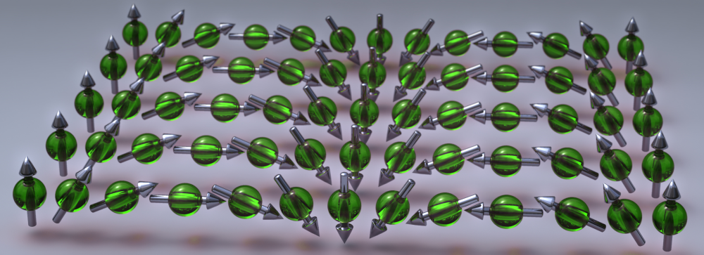
However, researchers have found that they can create textures by tuning the spin-orbit interactions so that they behave effectively like a unidirectional magnetic field throughout the material [2]. Such a field uniformly rotates the spins of all electrons that move across the material in a particular direction, regardless of whether an individual electron takes a straight path or a zigzag path due to scattering. This coordination between the electron motion and the spin rotation results in a spin texture called a persistent spin helix (PSH). The PSH state, which consists of regions of aligned spins that form stripes, has potential uses in spintronic devices such as spin field-effect transistors [3].
Researchers have shown that they can generate PSHs that last as long as a few nanoseconds—a long time by electron standards—by shining a beam of light onto a collection of electrons restricted to a single atomic layer in a semiconductor. The light aligns electron spins, and as these electrons diffuse outward from the beam location, they evolve into the PSH texture. “Because spin diffusion is required, it takes time to form the striped spin pattern using the typical method,” says Jun Ishihara from the Tokyo University of Science.
Ishihara and his colleagues have devised a more direct method using an optical vortex beam, whose polarization varies in a cyclical pattern around the beam’s dark central region. The number of polarization cycles around the beam axis is related to the orbital angular momentum of the vortex. By shining this beam onto a sample of the semiconductor gallium arsenide, the researchers imprinted a circular spin pattern into electrons in a layer within the material. The sizes of the patches of up and down spins in this initial pattern were similar to the stripe widths in the team’s desired PSH texture.
The researchers observed the resulting spin texture at later times using a probe beam that could detect electron spin orientation. They found that a pattern with 5-µm-wide stripes appeared in the semiconductor about 10 picoseconds after the vortex beam excitation, whereas the same striped pattern took 100 picoseconds to form when the team used a conventional laser beam. Ishihara and his colleagues also showed that, in addition to generating the PSH texture faster, a single vortex beam could create two PSH textures with opposite phases. Such spin control has not been demonstrated with ordinary beams.
“This work takes the optical manipulation of spin texture to the next level,” says spintronics expert Alan Bristow from West Virginia University. He says that the orbital angular momentum in the vortex beam can be made to match the natural spin oscillations in the electrons. “This work opens the door for further exploration of ultrafast optical manipulation of spin textures in semiconductor devices,” Bristow says.
–Michael Schirber
Michael Schirber is a Corresponding Editor for Physics Magazine based in Lyon, France.
References
- J. Ishihara et al., “Imprinting spatial helicity structure of vector vortex beam on spin texture in semiconductors,” Phys. Rev. Lett. 130, 126701 (2023).
- B. Andrei Bernevig et al., “Exact SU(2) symmetry and persistent spin helix in a spin-orbit coupled system,” Phys. Rev. Lett. 97, 236601 (2006).
- Y. Kunihashi et al., “Proposal of spin complementary field effect transistor,” Appl. Phys. Lett. 100, 113502 (2012).
More Information
A description of the persistent spin helix provided by the Japanese company NTT.


