




When Electrons Go Ballistic
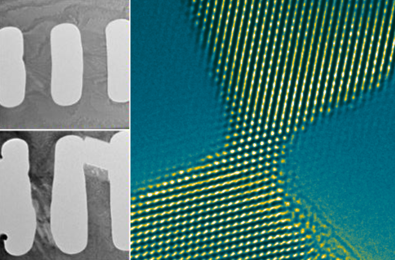

The current through a nanowire can have unique quantum characteristics arising from ballistic transport—the scattering-free flow of conduction electrons. To study the limits of this behavior, researchers have now built a “minilab” that accomplishes two measurements at once: It images a wire that is being deformed while also tracking its electrical conductance [1]. The team used the system to pinpoint the width of gold nanowires below which ballistic transport becomes operative. This work could help in the development of nanoscale switches and memory devices.
In a normal wire, the conduction electrons constantly ricochet off atoms in the material, creating resistance in the current flow. In very narrow wires, by contrast, the electrons can practically sail from one end to the other without scattering. ln the confined geometry of a nanowire, the electron wave function decomposes into a set of discrete modes, analogous to the standing waves of a guitar string, explains Xiaodong Han from the Southern University of Science and Technology in China. Each mode is like a channel in which electrons travel ballistically and for which the electrical conductance is fixed at a quantized amount. The value of this quantum of conductance is 2e2/h, where e is the charge of the electron and h is Planck’s constant.
This quantization leads to discrete levels in a nanowire’s conductance corresponding to the number of modes within the nanowire. Those levels could act as the 0’s and 1’s of a memory device called a memristor. The levels can, however, blur together when the wire becomes too wide, so researchers want to characterize the ballistic transport in nanowires as the width varies.
Previous experiments have used transmission electron microscopy (TEM) to image nanowires, but the challenge has been to relate changes in the observed width to changes in the wire’s electronic properties. Han and his colleagues built the all-in-one minilab with the capability to slowly stretch a nanowire while continuously monitoring its atomic structure and its conductance.
The researchers loaded their system with a gold foil containing cutout regions that created three parallel nanowires through which current could flow. Actuators in the device slowly pulled on the ends of the foil, forcing two of the nanowires to break. Further pulling caused the remaining nanowire to stretch out, creating a narrow “neck” that was initially about 250 nanometers (nm) wide. The rack-like stretching allowed the team to observe a range of different-sized structures within a single experimental run, thus avoiding potential systematic errors from combining data from multiple runs.
Using the minilab’s TEM capabilities, Han and his colleagues were able to track the width of the neck-like wire as it was stretched. At the same time, they measured the wire’s conductance using pairs of electrodes connected to the gold foil. The conductance dropped as the wire became narrower, and at a certain point, the conductance began to exhibit discrete steps, signaling that ballistic transport was occurring. As the atomic-resolution TEM images revealed, the critical width for this change was 2.5 nm, corresponding to a wire that was just 11 atoms wide at its narrowest point. The team continued to stretch the wire, revealing more discrete conductance steps, until the wire broke.
A critical size of 2.5 nm for ballistic transport is consistent with predictions that it should be significantly smaller than the distance traveled by conduction electrons in gold between scattering events (the mean free path). This distance is approximately 38 nm at room temperature. The critical width depends on the details of each metal, and Han points out that other materials may be more sensitive than gold to thermal fluctuations. To reduce the impact of such fluctuations, the team is planning to lower the temperature of their system with cryogenic cooling.
Han says that the data—specifically the measurements of the variation of the conduction with decreasing width—could help researchers designing devices. As an example, he mentions the quantum conductance atom switch, a device still under development that uses ballistic transport over atomic bridges [2]. These bridges can be formed and annihilated—turning the switch on and off, respectively—through mechanical or electrochemical processes.
Gianluca Milano, a memristor expert from the Polytechnic University of Turin in Italy, says that the researchers have provided a useful platform. “In general, understanding the ballistic transport in nanostructured devices opens the possibility of new applications of such systems.” Milano and his colleagues recently showed that ballistic transport might be exploited to create a new standard of resistance for the International System of Units (SI) [3].
–Michael Schirber
Michael Schirber is the Deputy Editor of Physics Magazine.
References
- X. Yang et al., “Approaching the ballistic transport limit in single crystalline Au,” Phys. Rev. Lett. 135, 216302 (2025).
- F.-Q. Xie et al., “Gate-controlled atomic quantum switch,” Phys. Rev. Lett. 93, 128303 (2004).
- G. Milano et al., “A quantum resistance memristor for an intrinsically traceable International System of Units standard,” Nat. Nanotechnol. (2025).