Spintronics without magnetism
The 2007 Nobel Prize in Physics (awarded to Albert Fert and Peter Grünberg) highlighted the remarkably rapid transition of “spintronics” from fundamental studies of spin-dependent transport in metallic ferromagnetic multilayers [1] to a device technology critical to the magnetic storage industry. While the mainstream of spintronics continues to expand the scientific and technological frontiers of ferromagnetic metal devices [2], a parallel effort in semiconductor spintronics is growing vigorously [3]. This incarnation of spintronics has the same general motivation as metallic spintronics: to understand and control the transport of spin-polarized currents and to eventually apply this knowledge in information technologies. However, semiconductor spintronics also brings with it the promise of integrating the best qualities of two disparate worlds: the unparalleled storage capacity of magnetic memory and the impressive computing power of semiconductor logic. Add to this the possibility of exploiting the relatively long-lived quantum coherence of spin states in semiconductors [4] and one can even imagine unleashing the full power of the quantum world in truly revolutionary devices that exploit both the amplitude and phase of wave functions. Needless to say, the realization of this potential requires concerted efforts aimed at both understanding the mechanisms for spin-dependent transport in semiconductors as well as critically comparing spin-based device schemes with existing technologies [5].
At first glance, it seems almost a given that ferromagnetism would be a necessary and integral component of any scheme for semiconductor spintronic devices. For instance, a semiconductor spintronic device generically requires an imbalance between spin “up” and “down” populations of electrons (or holes). We can imagine this imbalance being created by the injection of spin-polarized charge carriers from a ferromagnet, which acts as a spin polarizer. Alternatively, we could build devices from ferromagnetic semiconductors that have an intrinsic spin imbalance. Indeed, important advances have been made in semiconductor spintronics by using these very notions, with a number of interesting proof-of-concept semiconductor spintronic device demonstrations that incorporate ferromagnetic elements for injecting, detecting, and manipulating spins [6]. But, discoveries in recent years have inspired a completely different avenue to semiconductor spintronics—one that does not involve any ferromagnetism whatsoever [7–9].
The development of this alternate track—“spintronics without magnetism”—relies on our ability to manipulate carrier spins in semiconductors through the spin-orbit interaction. This is an attractive pathway for designing semiconductor spintronic devices because spin-orbit coupling enables the generation and manipulation of spins solely by electric fields. This is easy to understand in a qualitative way by recalling that spin-orbit coupling is the natural outcome of incorporating special relativity within quantum mechanics (the Dirac and Pauli equations). In the rest frame of an electron moving through a lattice, the external electric field (along with that from the atomic cores) is Lorentz transformed into a magnetic field that can act upon the spin of the electron. Using the spin-orbit interaction for manipulating electron spin obviates the design complexities that are often associated with incorporating local magnetic fields into device architectures. As we discuss below, the basic conceptual framework for the influence of the spin-orbit interaction on mobile electron spins has deep and old roots, but the experimental harnessing of these concepts is very contemporary and still at an early—and exciting—stage of development and discovery.
The spin-orbit coupling generates spin polarization through two conceptually different processes: spin-dependent scattering and the acquisition of a geometric phase. The former idea harks back to the heyday of quantum mechanics, when Sir Neville Mott first used the Dirac equation to calculate the spin-dependent skew scattering of relativistic electrons by a Coulomb potential, in which electrons with spin up and down are scattered in opposite trajectories [10]. Mott’s argument has now resurfaced within condensed matter physics in the anomalous [11] and spin Hall effects [12]. Further, band-structure effects provide variations on this interplay between scattering and the spin-orbit interaction by the removal of spin degeneracy in momentum space [13–15]. This removal of spin degeneracy acts like an “effective magnetic field” that can be engineered into a semiconductor crystal by using factors such as strain.
The second means of manipulating spins via spin-orbit coupling can be traced back conceptually to Pancharatnam’s early work on geometrical phases in the polarization of light [16]—later rediscovered within the context of spins by Michael Berry [17]. Several recent proposals have now shown how transported spins can acquire a geometric—or “topological”—phase in the presence of unusual band structures [18,19].
In this article, we focus our discussion on experiments that examine the first, largely “extrinsic” means of spin control wherein impurity scattering plays a key role, referring the reader to more recent perspectives [20] on experiments [21] that have addressed the topological methodologies of generating spin polarization in semiconductors.
Experiments show that when an “ordinary” current flows through an “ordinary” semiconductor, spin polarization arises from two complementary effects that often coexist: the spin Hall effect and current-induced spin polarization. Remarkably, both these phenomena are observable in a variety of standard semiconductor crystals, ranging from bulk (three-dimensional) samples to exquisitely designed two-dimensional electron gases (2DEGs). Once a spin-polarized current is generated in a semiconductor, we can use the spin-orbit interaction to further modulate this spin polarization by taking advantage of symmetry-breaking factors such as interfaces, electric fields, strain, and crystalline directions. The techniques for accomplishing this are now well understood and are based upon the key insights provided by the pioneering work of Dresselhaus, Rashba, and others [13–15]. Indeed, the seminal proposal for a semiconductor spintronic device by Datta and Das [22] derived its essential functionality from the electric field-controlled precession of injected electron spins (the Rashba effect). As we discuss below, experiments have now revealed a vast playground in which the spin-orbit interaction may be exploited for spin precession control, including strain-engineered architectures and epitaxial crystalline orientation.
The spin Hall effect
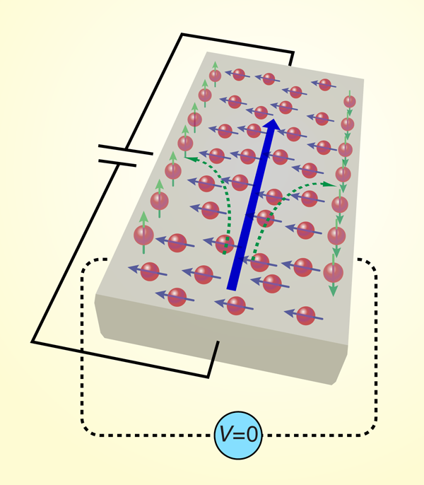
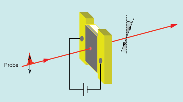
The spin Hall effect arises when a current flows through a semiconductor in the presence of a spin-orbit interaction, creating spin accumulation at the edges of a semiconductor transport channel (green arrows, Fig. 1). Though predicted over thirty years ago [12], unambiguous experimental evidence for the spin Hall effect required the development of high-sensitivity scanning optical imaging techniques capable of detecting small (microradians) Kerr rotation of reflected linearly polarized light (illustrated in Fig. 2) [7]. The technique has now been used to directly visualize the steady-state spin accumulation from the spin Hall effect of conduction-band electrons in several three-dimensional semiconductor crystals— and [7] and [23]—as well as in 2DEGs [24]. In addition, the optical nature of the measurement lends itself to spatiotemporally resolved pump-probe measurements that image the accumulation, precession, and decay dynamics near the channel boundary and provide insights into the dynamical evolution of the spin Hall effect (revealing, for instance, multiple time constants) [25].
The early experiments reporting the spin Hall effect ignited a surge of theoretical interest in the phenomenon, raising fundamental questions about its microscopic origins [26,27], the nature of spin currents [28,29], and the behavior of electrically generated spin accumulation in micron-scale devices [30,31]. The imaging experiments provide clear answers to some of these debates, demonstrating the clearly extrinsic nature of the spin Hall effect of electrons in all samples studied so far and also verifying the drift-diffusion dynamics of electrically generated spins in micron-scale devices [32,33]. When coupled with “Hanle measurements” that determine the precessional spin dephasing in an orthogonal magnetic field, the imaging experiments also provide a way to estimate the magnitude of the effect in terms of a “spin Hall conductivity.” Theoretical analysis of the extrinsic spin Hall effect in semiconductors using a spin-dependent Boltzmann approach provides good agreement with the experimentally measured spin Hall conductivity [33]. It is also apparent from both experimental measurements and theory that the spin Hall conductivity should depend both on the spin-orbit coupling parameter (characteristic of the semiconductor host band structure) and the gradient of the impurity scattering potential (in other words, the local electric field).
Nonetheless, key experimental observations still remain largely unanswered, for instance, although the extrinsic spin Hall effect in is rapidly quenched with increasing temperature (observable up to about ), experiments readily show the spin Hall effect at room temperature in despite the fact that the spin-orbit coupling parameter is much weaker in this material [23]. This temperature dependence is still a mystery that needs to be resolved. Further, the magnitude of the spin Hall effect in all the materials studied is still too small to envisage even proof-of-concept semiconductor devices that exploit the phenomenon and it is not clear what parameters could be manipulated for enhancing the signal. Addressing these questions provides an important challenge of both fundamental and technological implications.
Current-induced spin polarization
As we mentioned above, the spin Hall effect is often accompanied by another spin polarization effect associated with a flowing charge current: bulk spin polarization generated by electron currents. As with the spin Hall effect, this effect in semiconductors with spin-orbit coupling was predicted decades before being confirmed by experiments [15,34]. Unlike the spin Hall effect, the spin polarization associated with this effect is larger, with a spatially uniform distribution and oriented in directions that depend on detailed device and crystal geometry (blue arrows, Fig. 1). This phenomenon has been called “current-induced spin polarization” and has also been observed in several semiconductors and geometries [9,23–25,35].
Current-induced spin polarization of conduction electrons was observed using Kerr rotation in strained semiconductors [9]. By studying the current-induced spin polarization in 2DEG devices fabricated along different crystalline directions for the current channel [25], we can disentangle contributions from “Rashba” and “Dresselhaus” fields (the distinction between the two is described in more detail below). Many of the experimental observations, such as the dependence of the spin polarization on the direction of the current density and electric field, can be understood as arising from these spin-orbit fields. However—as in the case of the spin Hall effect—we still do not have a sufficient understanding of the phenomenon that would provide guidelines for designing materials with favorable parameters. For instance, in contrast to -type , current-induced spin polarization can be observed in -type at room temperature [23]. The picture is further complicated by the poor correlation between the magnitude of current-induced spin polarization and the measured spin splittings in [9] and competing proposals for spin-orbit mechanisms to describe this phenomenon [36]. These open theoretical questions combined with the potential utility of a spontaneous bulk electrically induced spin polarization present important outstanding challenges for spin-orbit physics in semiconductors.
Spin manipulation via “effective magnetic fields”
So far, we have addressed the generation of spin polarization by a current. How can we manipulate the direction of this polarization once it has been created? The Rashba and Dresselhaus internal magnetic fields again come to our aid: the former originate in a spin-splitting in strained semiconductors that varies linearly with , the crystal momentum, while the latter have a cubic dependence on crystal momentum. These -dependent spin splittings act on spins in semiconductors as if they were “effective magnetic fields” that depend on the motion of charge in the material. Since similar spin splittings can be induced by strain in crystals, strain-engineered heterostructures provide a powerful means of systematically designing these internal magnetic fields, thus yielding means of using the spin-orbit coupling to manipulate spins. In analogy to real applied magnetic fields, strain-induced effective fields have been used for both coherent spin precession and electrically-driven spin resonance [8]. The internal magnetic field has been used for manipulating spin transport in , , and devices [37,38]. Although the spin-orbit coupling parameter is much smaller in compared to , the spin-splitting energy scale is surprisingly comparable. The potential for all-electrical spintronics has been demonstrated in structures where precession of current-induced spin polarization is caused by strain-induced spin splittings, all in a single device without real magnetic fields or magnetic materials [36].
Finally, a very exciting development in recent years is the realization that one can engineer the interplay between the Rashba and Dresselhaus terms in 2DEGs, yielding spin polarization waves that survive over length scales substantially longer than predicted by diffusive dynamics alone. This phenomenon arises because the relationship between real-space trajectory and spin precession leads to a correlation between the electron’s position and its spin, resulting in an enhancement of the lifetime of certain spatially inhomogeneous spin polarization states beyond what would be expected for conventional spin diffusion—a spin helix. Recent optical transient spin-grating spectroscopy experiments [39] have probed the relaxation rates of spin polarization waves in 2DEGs and shown that the spin polarization lifetime is maximal at a nonzero wave vector. This is contrary to expectations based on ordinary spin diffusion, but in quantitative agreement with recent theories that treat diffusion in the presence of spin-orbit coupling. Balancing the Rashba and Dresselhaus terms may enable modulation of the spin correlation length, with large dynamic range, through the application of external electric fields.
In summary, new pathways are emerging for exploiting the spin-orbit interaction to generate and manipulate carrier spin polarization in semiconductors. The wealth of experimental data gathered in recent years has clearly identified phenomena such as the spin Hall effect, current-induced spin polarization, and the spin helix [40] that could very well form the underpinnings of “spintronics without magnetism.” Bridging the chasm between fundamental understanding and a viable technology still remains a daunting challenge, but also offers stimulating scientific opportunities for quantum engineering at the very frontiers of condensed matter physics.
References
- E. Y. Tsymbal and D. G. Pettifor, in Solid State Physics Vol. 56, edited by Frans Saepen and Henry Ehrenreich (Academic, New York, 2001), p. 113[Amazon][WorldCat]
- D. C. Ralph and M. D. Stiles, J. Magn. Magn Mater. 320, 1190 (2008)
- Semiconductor Spintronics and Quantum Computation, edited by D. D. Awschalom, D. Loss, and N. Samarth (Springer, Berlin, 2002)[Amazon][WorldCat]
- J. M. Kikkawa and D. D. Awschalom, Nature 397, 139 (1999)
- K. C. Hall and M. E. Flatté, Appl. Phys. Lett. 88, 162503 (2006)
- D. D. Awschalom and M. E. Flatté, Nature Phys. 3, 153 (2007)
- Y. K. Kato, R. C. Myers, A. C. Gossard, and D. D. Awschalom, Science 306, 1910 (2004)
- Y. Kato, R. C. Myers, A. C. Gossard, and D. D. Awschalom, Nature 427, 50 (2004)
- Y. K. Kato, R. C. Myers, A. C. Gossard, and D. D. Awschalom, Phys. Rev. Lett. 93, 176601 (2004)
- N. F. Mott, Proc. R. Soc. London A 124, 425 (1929)
- N. Nagaosa, J. Phys. Soc. Japan 75,042001 (2006)
- M. I. D’yakonov and V. I. Perel, JETP Lett. 13, 467 (1971)
- G. Dresselhaus, Phys. Rev. 100, 580 (1955)
- Y. A. Bychkov and E. Rashba, J. Phys. C 17, 6039 (1984)
- A. G. Aronov, Yu. B. Lyanda-Geller, and G. E. Pikus, Sov. Phys. JETP 73, 537 (1991)
- S. Pancharatnam, Proc. Indian Acad Sci. A 44, 247 (1956)
- M. V. Berry, Proc. R. Soc. London A 392, 45 (1984)
- B. A. Bernevig, T. L. Hughes, and S.-C. Zhang, Science 314, 1757 (2006)
- L. Fu, C. L. Kane, and E. J. Mele, Phys. Rev. Lett. 98, 106803 (2007)
- J. Zaanen, Science 323, 888 (2009)
- M. König et al., Science 318, 766 (2007)
- S. Datta and B. Das, Appl. Phys. Lett.56, 665 (1990)
- N. Stern, S. Ghosh, G. Xiang, M. Zhu, N. Samarth, and D. D. Awschalom, Phys. Rev. Lett. 97, 126603 (2006)
- V. Sih, R. C. Myers, Y. K. Kato, W. H. Lau, A. C. Gossard, and D. D. Awschalom, Nature Phys. 1, 31 (2005)
- N. P. Stern, D. W. Steuerman, S. Mack, A. C. Gossard, and D. D. Awschalom, Nature Phys. 4, 843 (2008)
- J. Sinova, D. Culcer, Q. Niu, N. A. Sinitsyn, T. Jungwirth, and A. H. MacDonald, Phys. Rev. Lett. 92, 126603 (2004)
- H. Engel, B. I. Halperin, and E. I. Rashba, Phys. Rev. Lett. 95, 166605 (2005)
- J. Shi, P. Zhang, D. Xiao, and Q. Niu, Phys. Rev. Lett. 96, 076604 (2006)
- V. Sih, W. H. Lau, R. C. Myers, V. R. Horowitz, A. C. Gossard, and D. D. Awschalom, Phys. Rev. Lett. 97, 096605 (2006)
- W.-K. Tse, J. Fabian, I. Zutić, and S. Das Sarma, Phys. Rev. B 72, 241303 (2005)
- N. P. Stern, D. W. Steuerman, S. Mack, A. C. Gossard, and D. D. Awschalom, Appl. Phys. Lett. 91, 062109 (2007)
- V. Sih, W. H. Lau, R. C. Myers, V. R. Horowitz, A. C. Gossard, and D. D. Awschalom, Phys. Rev. Lett. 97, 096605 (2006)
- H. Engel, B. I. Halperin, and E. I. Rashba, Phys. Rev. Lett. 95, 166605 (2005)
- E. L. Ivchenko and G. Pikus, JETP Lett. 27, 604 (1978)
- A. Yu. Silov et al., Appl. Phys. Lett. 85, 5929 (2004)
- H. A. Engel, E. I. Rashba, and B. I. Halperin, Phys. Rev. Lett. 98, 036602 (2007)
- Y. K. Kato, R. C. Myers, A. C. Gossard, and D. D. Awschalom, Appl. Phys. Lett. 87, 022503 (2005)
- S. Ghosh, N. Stern, B. Maertz, D. D. Awschalom, G. Xiang, M. Zhu, and N. Samarth, Appl. Phys. Lett. 89, 242116 (2006)
- C. P. Weber, J. Orenstein, B. Andrei Bernevig, Shou-Cheng Zhang, Jason Stephens, and D. D. Awschalom, Phys. Rev. Lett. 98,076604 (2007)
- J. D. Koralek, et al., Nature 458, 610 (2009)