Geodesic carbon nanodomes
Graphene has been attracting tremendous attention ever since its discovery in 2004 [1] largely because of its fascinating electronic properties. Among these are high electron mobility at room temperature that is mostly independent of doping, and carriers that behave like massless Dirac fermions [2]. Graphene consists of a single layer of graphite, a honeycomb array of carbon atoms, and was first prepared by mechanically stripping a single layer from a graphite crystal. Harnessing the potential of graphene in electronic devices, however, requires a method for producing it in sizes larger than available graphite crystals, and surface scientists have been concentrating on developing methods of producing large-scale and perfect graphene films.
Various methods have been employed to fabricate graphene films, primarily (i) epitaxial growth, which involves the deposition of carbon onto a substrate that has a good lattice match with graphene or by thermal decomposition of SiC [3]; (ii) self-assembly procedures in which graphene oxide films are produced in solution and then transferred to a substrate and reduced to graphene by chemical reaction or heating [4]; and (iii) chemical vapor deposition, in which hydrocarbon gases are adsorbed on a hot surface, and which has been shown recently to produce large high-quality graphene films on metal surfaces, which can then be transferred intact to other substrates [5,6].
In a paper in Physical Review Letters, Paolo Lacovig, Monica Pozzo, Dario Alfè, Paolo Vilmercati, Alessandro Baraldi, and Silvano Lizzit at institutions in Italy, the UK, and the US report photoelectron spectroscopy data that suggests that en route to forming continuous sheets, graphene islands grow on an iridium surface in the form of microscopic domes [7]. According to their model, the domes consist of circular islands of graphene that are attached via strong chemical bonds to the close-packed iridium surface at the island’s perimeter, but are not chemically attached in the center. The islands grow by attaching atoms and smaller islands to their edges.
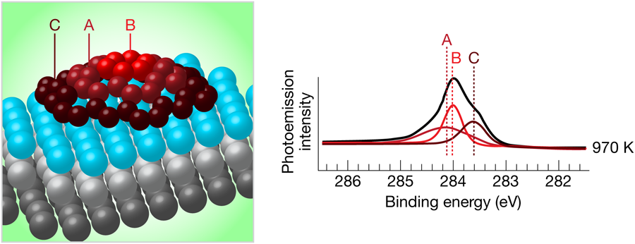
To characterize these islands, the authors used high-resolution photoelectron spectroscopy, which produces a spectrum of the core electronic energy levels present in the atoms at the surface. These energy levels are sensitive to the chemical environment of the atom, and, for instance, are different for iridium atoms deep in the bulk compared to iridium atoms at the surface. Likewise, carbon atoms in different bonding configurations at the surface will have different electronic energy levels (see Fig. 1).
Lacovig et al. used two different methods to grow their graphene islands. The first, temperature-programmed growth, involved the adsorption of C2H4 at room temperature, followed by sequential heating to successively higher temperatures. For heating temperatures below 1000K, the single electronic peak for carbon electrons having a binding energy of about 284eV is split into three components. After heating to higher temperatures, two of the components gradually shift and disappear, while the third one grows, and after heating to 1270K, only one peak remains. At the same time, an additional peak appears in the spectrum of Ir electrons for the low-temperature anneals, but gradually disappears as the annealing temperature is increased.
These results were interpreted with the help of density-functional-theory calculations that considered different sizes of graphene clusters on iridium. These calculations clearly showed that the interaction of the carbon atoms with the iridium substrate is much larger at the edges of the island than in the center, and that as the islands grow larger, the central carbons detach and move away from the substrate, creating a dome-shaped island. For very large islands, almost all of the carbon atoms are in this nearly-free-standing state, and only the ones at the perimeter of the islands are strongly bound to the surface. This scenario matches the experimental findings, indicating an evolution, as a function of the heating temperature, from small graphene islands in which carbon atoms have several different chemical environments to very large islands that approach free-standing graphene.
For islands grown with chemical vapor deposition, the substrate was held at a constant high temperature in the range 820– 1270K. At this temperature, the graphene grows over large areas, consistent with the first method where the heating temperature was high, except that an extra peak was observed in the carbon photoemission spectrum that was attributed to carbon atoms at step sites of the substrate. The higher occupation of substrate step sites for samples grown with this method was also observed in an earlier scanning tunneling microscopy experiment [8] and was attributed to the higher mobility of the carbon atoms on the surface, allowing them to diffuse and stick to the step sites, and thereby nucleating the graphene growth.
The two methods of growth produce graphene layers having different characteristics. Using temperature-programmed growth, the graphene forms nanoislands with sizes that are controllable by adjusting the heating temperature, from a few nm to hundreds of nm. The ability to control the island size opens the possibility of investigation of the quantum confinement of the massless charge carriers in graphene, and to further investigate the details of properties and the catalytic growth process at the edges of the islands. With chemical vapor deposition, the whole surface can be covered with a sheet of graphene. Since this is a method that is readily available on an industrial scale, there is potential for incorporating high-quality macroscopic graphene films in electronic devices.
Remarkably, these results suggest that the Ir(111) surface catalyzes the growth at the edges of the graphene islands, and that hydrogen does not play any active role in the formation of the graphene films. The picture presented is one where free carbon atoms and small carbon clusters that result from the hydrocarbon decomposition diffuse on the surface to form the islands. It will be very interesting to explore the release of hydrogen as the hydrocarbon molecules react to form graphene. This process would leave islands that are hydrogen terminated without dangling bonds that bind to the metallic surface, producing flat graphene even for small islands. If controlled experiments can produce films having different amounts of hydrogen, then the ability to fabricate films that include both conducting graphene and insulating “graphane”—a two-dimensional layer of covalently bonded hydrocarbon [9]—cannot be far behind. With this ability, the possibilities of producing graphene electronic devices, controlling the work function and optical properties of these materials are endless. Graphene layers might then replace much thicker layers currently used in electronic microcircuits, making future computers and other devices more compact and energy efficient.
References
- K. S. Novoselov, A. K. Geim, S. V. Morozov, D. Jiang, Y. Zhang, S. V. Dubonos, I. V. Grigorievea, and A. A. Firsov, Science 306, 666 (2004)
- A. K. Geim, Science 324, 1530 (2009)
- C. Berger, Z. Song, T. Li, Z. Li, A. Y. Ogbazghi, R. Feng, Z. Dai, A. N. Marchenkov, E. H. Conrad, P. N. First, and W. A. de Heer, J. Phys. Chem. 108, 19912 (2004)
- X. Li, G. Y. Zhang, X. D. Bai, X. M. Sun, X. R. Wang, E. Wang, and H. J. Dai, Nature Nanotech. 3, 538 (2008)
- K. S. Kim, Y. Zhao, S. Y. Lee, J. M. Kim, K. S. Kim, J. H. Ahn, P. Kim, J. Y. Choi, and B. H. Hong, Nature 457, 706 (2009)
- X. Li, W. Cai, J. An, S. Kim, J. Nah, D. Yang, R. Piner, A. Velamakanni, I. Jung, E. Tutuc, S. K. Banerjee, L. Colombo, , and R. Ruoff, Science 324, 1312 (2009)
- P. Lacovig, M. Pozzo, D. Alfè, P. Vilmercati, A. Baraldi, and S. Lizzit, Phys. Rev. Lett. 103, 166101 (2009)
- J. Coraux, A. T. N’Diaye, M. Engler, C. Busse, D. Wall, N. Buckanie, F. J. M. zu Heringdorf, R. van Gastel, B. Poelsema, and T. Michely, New J. Phys. 11, 023006 (2009)
- J. O. Sofo, A. S. Chaudhari, and G. D. Barber, Phys. Rev. B 75, 153401 (2007)


