Best of both worlds?
The integration of optical circuits and conventional silicon devices would make it possible to synchronize multiple processors on a chip by means of light pulses. Unfortunately, the same silicon that underpins the vast CMOS (complementary metal-oxide-semiconductor) industry is only a mediocre light emitter.
The emission from nanocrystalline silicon is enhanced by quantum confinement, but the efficiencies are still marginal. As Yiyang Gong and colleagues at Stanford University in the US, in collaboration with Toshiba Corporation, Japan, report in Physical Review B, a route toward integrated silicon photon circuitry may lie in combining nanocrystal structures with photonic crystal nanocavities to boost light emission. Their work also identifies the barriers still to be overcome.
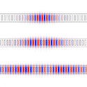
Photonic crystals are structures in which regular nanopatterning creates optical band gaps—frequency regions where light cannot propagate in the material. Resonant cavities made from photonic crystals could, in principle, promote radiative decay modes at the expense of useless nonradiative modes. Gong et al. find that silicon nanocrystals embedded in a silicon dioxide host matrix, when coupled to a high-quality-factor photonic crystal cavity, indeed show promise as fully CMOS compatible photonic elements, but they also point to photon absorption by free carriers as a drawback that needs attention. – David Voss


