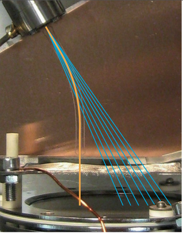
Integrated circuits for matter waves
In the second half of the th century, miniaturization and integration were crucial to develop the electronics that formed the backbone of the information revolution. Since the 1990s, scientists have applied the same methods to manipulating quantum objects on a chip [1]. One of the first examples was the atom chip [2], which combined the best of two worlds—the quantum manipulation techniques that have been perfected by atomic physicists and the powerful toolbox of nanofabrication. Since then, ions [3] and molecules [4] have joined the ranks. Now, borrowing techniques from atom, ion, and molecular chips, Johannes Hoffrogge and co-workers [5] at the Max Planck Institut für Quantenoptik in Garching, Germany, in collaboration with Stanford University, demonstrate that electrons can also be guided in an analogous fashion. Writing in Physical Review Letters, they show they are able to control the path of electrons along a miniaturized linear quadrupole guide fabricated on a chip (Fig. 1). This demonstration constitutes an important step towards integrated electron optics and matter-wave interferometry [6].
Atom chips have already made it much easier to create degenerate quantum matter experimentally [1]. The chips rely on surface-mounted microstructures, ranging in scale from several hundreds of microns down to submicron size. These structures, of different shapes and sizes, are tailored to generate magnetic and electric fields that allow the atoms to be manipulated close to the chip surface. The structures are robust, as demonstrated in free-falling experiments in a drop tower [7], promising as a time reference [8], and employed for trapped atom interferometry [9].
In addition to robustness, in order to have maximum control over a quantum particle’s path, these trapping and guiding structures should enforce occupation of only a single (transverse) mode, as in fiber optics for light. As such, the confining potential produced by the electric and magnetic fields needs to be very steep, that is, have strong gradient in the direction orthogonal to the guiding, to achieve a transverse energy level spacing that is larger than the thermal energy of the particles. It is interesting to note that although one needs strong confinement, that is, a potential minimum with a large curvature (large second derivative ) for single-mode operation, the confining potentials do not need to be deep. Strong gradients and curvatures are found close to the source of the fields—electric charges or currents—which leads naturally to miniaturization of the quantum devices. With moderate electric charges or currents, one can hence create very tight traps of moderate trap depth and small volume. The challenge is then to load atoms, ions, or other particles into these small traps.
For particles exhibiting a magnetic or electric dipole, static dc fields can be used for trapping: Magnetic microtraps for neutral atoms can be created by current-carrying structures; electric microtraps for polar molecules can be created by charges. The atoms or molecules are then trapped in their weak field seeking state in a minimum of the external field.
Trapping potentials for charged particles such as ions or electrons have to rely on alternating ac fields or the combination of electric and magnetic fields [10].
One example of a trap for electrons and ions used in many experiments is the Penning trap, where the particle confinement is given by the interplay between the orbits in a magnetic field and an electric quadrupole field. Penning traps are very well suited for metrology experiments and are employed in the most precise mass measurements (measuring the charge-to-mass ratio), and in tests of QED through measuring magnetic moments and . Trapping electrons in microstructured Penning traps that combine a static external magnetic field with the electric field generated by a planar electrode geometry on a chip has recently been demonstrated [11].
The second possibility is the Paul trap, a three-dimensional trap, where the confinement of charged particles relies on the time-averaged action of an oscillating electric quadrupole field [10]. Trapping and guiding is stable if the motion of the confined particles is slow compared to the drive frequency . The stability can be characterized by the dimensionless parameter ), where is the charge-to-mass ratio of the trapped particles, is the amplitude of the oscillating voltage, and is the distance to the charged electrodes forming the quadrupole potential. For a very elongated trap or guide, stable transverse confinement is provided for . For small , the resulting pseudopotential is characterized by a frequency . One immediately sees that for constant and the trapping frequency scales like , and miniaturization helps in obtaining strong transverse confinement. This was the driving force behind miniaturizing ion traps, and the development of planar ion traps and the ion chip. Even though there are plenty of experiments with electrons in Penning traps, the confinement of electrons in the purely electric field of a Paul trap has rarely been considered. This is what the team of Hoffrogge et al. used.
To integrate a guide for electrons on a chip, one has to design a planar electrode configuration that creates a quadrupolar field. This can be done in analogy to the recently developed planar ion traps, but electrons, which have four orders of magnitude higher ratio, require significantly different driving parameters to keep small and at the same time generate a sufficiently large potential depth and transverse confinement. Hoffrogge et al. used a simple five-electrode configuration. The quadrupole field generated is only perfect at the center, but nevertheless there is a large enough region where the effective pseudopotential creates a tight but only moderately deep trap. It is interesting to note that the wire configuration is compatible with on-chip microwave transmission line technology to feed the structure the required microwave frequency oscillating electric field. For the wire configuration used, and a driving frequency of , and the maximum peak voltage of (corresponding to of power), the guiding potential is located above the central electrode and deep. The transverse confinement is . Scaling to a guide-to-surface distance of and a driving frequency of would result in a system providing even faster dynamics at a transverse frequency of .
In their experiments, Hoffrogge et al. are able to confine (in the traverse direction) and guide a low-energy electron beam of several electron volts along a - -long circular section of such a miniaturized linear quadrupole guide. Applying a microwave voltage to the electrodes fabricated on a planar substrate—the chip—generates the guiding potential.
The electrons propagate close to the surface and are subject to fluctuating surface fields, which results in heating. Typical heating rates are estimated to be a few quanta per second for room-temperature chip structures. Heating is a challenge also faced by microfabricated ion traps on chips, and can, in principle, be overcome by careful material choice and design, and by cooling the chip to cryogenic temperatures.
These beautiful experiments show a path towards detailed quantum control of electrons without the disturbing influences of the solid and thus open the door to many possibilities.
With a planar electrode configuration on a chip, one can generate complex wave guiding elements with the potential landscape precisely shaped on a microscopic scale. A new, guided, matter-wave system might result, with applications ranging from electron interferometry to novel noninvasive electron microscopy.
A further advantage of expanding Hoffrogge et al.’s experiments is that they will benefit significantly from novel electron sources, for example, ultrasharp tips culminating in a single atom that act as Heisenberg uncertainty limited point emitters [12]. By using electron optics that preserve phase-space density, it should be possible to directly transfer all electrons originating from a single-atom tip into the transverse ground state of the guiding potential, in close analogy to light guided in single-mode optical fibers. Appropriately structuring the guide will allow for the coherent splitting and recombination of an electron beam, which is needed in matter-wave interferometry experiments. In combination with the femtosecond controlled electron emission from these single atom tips [13], this will allow full spatial and temporal control of guided electrons. One can even think of coupling different guides to create entangled currents, or using trapped/guided electrons for quantum information processing.
References
- Atom Chips, edited by J. Reichel and V. Vuletic (Wiley-VCH, Weinheim, 2011)[Amazon][WorldCat]
- Ron Folman, Peter Krüger, Donatella Cassettari, Björn Hessmo, Thomas Maier, and Jörg Schmiedmayer, Phys. Rev. Lett. 84, 4749 (2000)
- D. Kielpinski, C. Monroe, and D. J. Wineland, Nature 417, 709 (2002)
- Samuel A. Meek, Horst Conrad, and Gerard Meijer, Science 3241699 (2009)
- J. Hoffrogge, R. Fröhlich, M. A. Kasevich, and P. Hommelhoff, Phys. Rev. Lett. 106, 193001 (2011)
- A. Cronin, J. Schmiedmayer, , and D. Pritchard, Rev. Mod. Phys. 81, 1051 (2009)
- T. van Zoest et al., Science 328, 1540 (2010)
- C. Deutsch et al., Phys. Rev. Lett. 105, 020401 (2019)
- T. Schumm et al., Nature Phys. 1, 57 (2005)
- F. G. Major, V. N. Gheorghe, and G. Werth, Charged Particle Traps (Springer, Berlin, 2005)[Amazon][WorldCat]
- P. Bushev et al., Eur. Phys. J. D 50, 97 (2008)
- P. Hommelhoff, Y. Sortais, A. Aghajani-Talesh, and M. A. Kasevich, Phys. Rev. Lett. 96, 077401 (2006)
- P. Hommelhoff, C. Kealhofer, and M. A. Kasevich, Phys. Rev. Lett. 97, 247402 (2006)