Better transistors through quantum mechanics
As chip designers seek to pack more transistors onto every square millimeter of silicon real estate, they run up against a fundamental problem: small devices become overwhelmed by quantum effects. However, some researchers are seeking to turn the tables by pressing quantum mechanics into service as part of the transistor design. In a paper in Physical Review B, Adam Sciambi of Stanford University, California, and his collaborators report their proof-of-principle experiments on a new kind of quantum transistor.
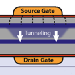
The team has created a two-layer quantum well heterostructure, in which the wave function of one layer extends into the second to modulate the tunneling current between the layers. In this design, a voltage on the first quantum well causes that layer to be depleted of carriers, which changes the subband energy level in the well. As the subband energy approaches the top of the quantum well potential, the wave function extends further and further out toward the second layer. When the wave function overlaps the second layer, the tunneling current can increase as much as two orders of magnitude, a substantial degree of gating leverage.
Although the reported design only works at cryogenic temperatures, a different choice of materials, for example, graphene, may allow operation at more technologically relevant temperatures. – David Voss


