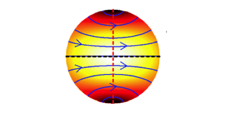
A New Window on Nanometer Apertures
Several precision optical techniques, such as high-resolution near-field scanning microscopy, depend on nanometer-sized holes to guide electromagnetic waves. Scientists have studied diffraction through subwavelength apertures since the th century, yet despite extensive effort, theory has not entirely accounted for the electromagnetic behavior of holes in real metals with finite thicknesses and dielectric constants. In a paper in Physical Review Letters, Juemin Yi, at the University of Strasbourg, France, and colleagues wrap up the problem in a complete package of theory and experiment.
Apertures large compared to the wavelength of electromagnetic waves yield their secrets to a rather straightforward theoretical approach, but when the holes become close to or smaller than the wavelength, the calculations become trickier. Moreover, experimental study is complicated by actual physical implementations involving real materials with a finite thickness rather than infinitely thin metal plates. Yi et al. conducted experiments in which they measured the full diffraction patterns of a circular aperture all the way from large holes down to subwavelength openings in realistic structures.
To accurately understand their observations, the authors find that not only do collective electron oscillations—the surface plasmons—need to be dealt with, but the interaction of the plasmons with waveguide modes of the aperture have to be included. Yi et al. derive a set of simple expressions that make it more straightforward to estimate the total transmission of light through a hole from measurements made along a single direction, as opposed to having to integrate over a wide range of angles. – David Voss


