Landmarks: Birth of Modern Electronics
Focus Landmarks feature important papers from the archives of the Physical Review.
In June 1948, the Physical Review published a description of a novel electronic device that “may be employed as an amplifier, oscillator, and for other purposes for which vacuum tubes are ordinarily used.” That statement hardly begins to capture the importance of the transistor, which made possible technology unimaginable at the time. But the first transistor design never saw commercial success. A different design, unveiled two years later by a colleague and rival of the original authors, spawned the modern microelectronics revolution.
Transistor inventors John Bardeen and Walter Brattain, of Bell Labs in New Jersey, described their device as a semiconductor triode. The triode was a vacuum tube with a metal “grid” interposed between a heated cathode that emitted electrons and an anode, the collector, to which those electrons traveled. Applying an electric potential to the grid would either enhance or diminish the electron flow, so that the triode functioned as an amplifier in which a small voltage controlled a large current.
Through the 1930s scientists were beginning to understand semiconductors, whose electrical properties depend crucially on impurities. In so-called n-type semiconductors, some electrons could hop from atom to atom, carrying a current. In p-type semiconductors, electricity flowed when the absence of an electron–a positively-charged “hole”–was able to migrate.
William Shockley, who supervised Bardeen and Brattain, proposed that a positive voltage applied to a metal plate adjacent to an n-type semiconductor would increase current flow by mobilizing electrons, so that the plate would function something like the grid in a conventional triode. Trying this in 1945, he found no effect at all and assigned Bardeen and Brattain to figure out why.
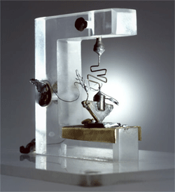
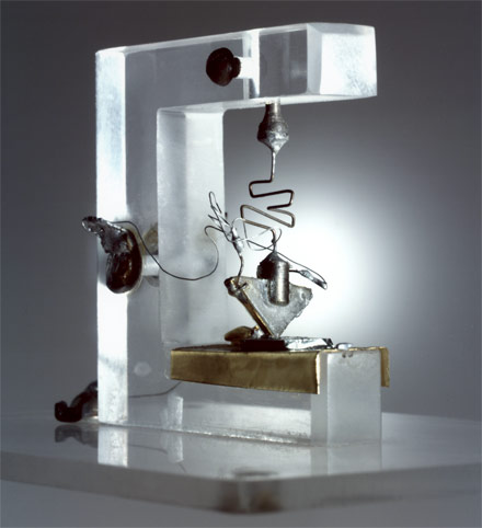
Bardeen and Brattain concluded that a thin p-type region formed at the surface below the plate, for reasons that were not entirely clear. After much trial and error, they built a semiconductor version of the triode that exploited this surface effect. They placed a slab of n-type germanium on a base electrode, then pressed two electrical contacts, a micron or two apart, onto its upper surface.
A small positive voltage (with respect to the base) applied to one of the upper contacts, dubbed the emitter, caused a flow of holes into the surface layer. Applying a negative potential to the other contact, the collector, drew the holes toward it, creating a current flow between the contacts. The emitter and collector had to be close together, Bardeen and Brattain found, for conditions at one to influence behavior at the other. A small variation in the emitter voltage then led to a large variation in the collector current and voltage, so that this “point-contact” device became an amplifier. Exactly how this transistor worked was somewhat mysterious, however, since understanding of hole and electron conduction in semiconductors was rudimentary at the time.
The device was demonstrated to Bell Labs staff in December, 1947, but didn’t appear in the Physical Review for another six months because of the need to establish a patent. An accompanying paper laid out evidence for the existence of the surface p-type layer [1].
Although Shockley had prompted Bardeen and Brattain’s research, he took little further interest in it, says Michael Riordan of the University of California, Santa Cruz, coauthor of a history of the transistor. Irked at their success, and believing that currents in the interior of the germanium as well as at its surface were important, Shockley set to work on a “junction” transistor, in which a thin layer of one type of semiconductor is sandwiched between slabs of the other type. This type of transistor, first demonstrated in 1950, depends crucially on “minority carriers”–holes flowing through an n-type material, or vice versa.
Announcement of the Bardeen-Brattain transistor drew considerable press attention, but it was an unreliable device, and the range of its possible applications was hard to foresee. Only when Shockley’s more reliable junction transistor went into commercial production did the enormous significance of the invention become apparent. The three men shared the 1956 Nobel Prize for physics.
–David Lindley
David Lindley is a freelance science writer, now retired. His most recent book is The Dream Universe: How Fundamental Physics Lost Its Way (Penguin Random House, 2020).
References
- W. H. Brattain and J. Bardeen, “Nature of the Forward Current in Germanium Point Contacts,” Phys. Rev. 74, 231 (1948)
More Information
Michael Riordan and Lillian Hoddeson, Crystal Fire: The Birth of the Information Age (Norton, 1997)
explanation of junction transistors from Hyperphysics
Transistorized! (TV show and web site on the history of the transistor)


