Straining After Quantum Dots
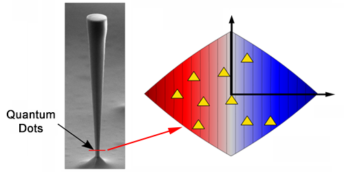
Several advanced optoelectronic devices, such as single-photon sources, are based on quantum dots embedded in micropillars or microwires. The quantum dots are typically produced via self-assembly processes and are thus randomly distributed within the microstructure. Pinpointing the exact positions of the dots in the material could greatly help the characterization and engineering of these devices. Now a team led by Julien Claudon, Maxime Richard, and Jean-Philippe Poizat at the University of Grenoble Alpes, France, has developed a technique that maps the dots’ positions by applying strain to the host structure and observing how this changes the dots’ photoluminescence.
The researchers demonstrated their approach with a wire-shaped antenna embedding a layer of indium arsenide quantum dots. Using a piezoelectrical transducer, they excited characteristic vibrational modes of the wire. These vibrations generated a strain field with a large gradient in the wire. Because the energy of the fundamental optical transition of the quantum dots is sensitive to strain, the wire oscillations resulted in time- and position-dependent shifts of the dots’ transition frequencies. The team characterized the effect by exciting the dots with a laser and measuring their photoluminescence spectra as a function of time. The analysis yielded a map of the positions of the dots inside the wire with an accuracy ranging between 1 and 35 nm, depending on the dots’ location with respect to the standing waves of the excited vibrational modes.
The authors suggest that their imaging method can be applied to any type of quantum system whose emission is strain-dependent, including quantum dots in semiconductor wires, nitrogen-vacancy centers in diamond, and rare-earth ions in crystals.
This research is published in Physical Review Letters.
–Matteo Rini
Matteo Rini is the Deputy Editor of Physics.


