3D Imaging of Dislocations
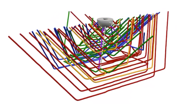
Dislocations are one of nature’s most elusive crystal defects. But new research from Daniel Hänschke at the Karlsruhe Institute of Technology, Germany, and colleagues [1] promises a way to unlock their secrets. The researchers combined several imaging techniques to provide a 3D view of a network of dislocations (Fig. 1) at an impressive level of detail and over an imaging volume that is orders of magnitude larger than that imaged with other techniques. This tool will be essential for understanding how these defects behave in industrially relevant materials. Such an understanding will become ever more important as electronic devices are manufactured on an increasingly smaller scale and to increasingly higher fault tolerances.
In a broad sense, crystals are defined by their regular arrangement of atoms, and it’s this arrangement that determines their properties. If a crystal has a structural defect, this can significantly (and often disastrously) change how it behaves. For example, a computer chip made from a crystal with a large density of defects might be more prone to failure, leakage currents that reduce the efficiency of the chip, or other unwanted side effects.
Defects in crystals are typically characterized by their dimensionality. The most common type of defect is a point defect. Such defects are not extended in any dimension, occurring at or around single atomic sites, where perhaps the atom is not where it should be. By contrast, dislocations are extended, one-dimensional defects. They are lines around which rows of atoms are misaligned, threading through the crystal much like strands of spaghetti. For example, an extra plane of atoms squeezed in where they shouldn’t be will terminate at a dislocation line. First described by Vito Volterra in 1907 [2], dislocations are now known to be crucial for understanding the mechanical properties of metals. This is mainly because they are fluid and dynamic. They can slip and glide through a crystal in response to stress, interact and become tangled with each other, and drag impurities or solutes along in their wake. Seminal work by Alan Cottrell and colleagues [3, 4] on iron with carbon additives showed how the clustering of carbon atoms around dislocations explains some of the very different properties of steels compared to plain iron: the carbon atoms help fix dislocations in place, increasing the amount of force necessary for the steel to yield. This understanding has revolutionized the ability to design new alloys for the modern world.
Despite their importance in metals, dislocations have long been under studied in nonmetals, such as the semiconductor materials from which computer chips, LEDs, and lasers are made. The reason for this is twofold. First, there are typically fewer dislocations in a semiconductor crystal than in a metal. This is because semiconductor crystals are grown more slowly and carefully, and also because semiconductors are not typically used as structural materials, and so are not subject to the stresses that can cause dislocations to multiply. Second, the dislocations themselves are also far less mobile in a semiconductor crystal than in a metal. However, we are learning that dislocations can be just as important to the properties of semiconductor devices as they are to those of metals. Also, as we reach the limits in performance of existing materials systems, we have to turn to materials that are more challenging to grow. These newer materials don’t have the benefits of decades of iterative innovation and optimization that silicon has had, and thus will have defect densities that are orders of magnitude higher. Therefore, we will need new techniques to properly characterize and understand dislocations in these materials. But even in silicon, dislocations are becoming more relevant, as a result of the relentless pursuit of Moore’s law to build increasingly smaller transistors on increasingly larger wafers. It is thus inevitable that defects such as dislocations will start to play a more important role.
The primary challenge is that dislocations are difficult to study. This is because they are associated with features on a wide range of length scales, from the atomic scale (the specific arrangement of atoms at the core of the dislocation) through to much larger scales (such as straining of the crystal far from the core, and how networks of dislocations interact with each other) [5]. This difference between length scales is huge: a powerful electron microscope that can image dislocation cores cannot “zoom out” far enough to give a larger, comprehensive picture of the defects. Also, some of the best techniques to image dislocations [6, 7] damage the sample, which is problematic if repeat measurements of a specific sample are desired.
Enter Hänschke and colleagues. The researchers combined several microscopy techniques—involving x rays (laminography and x-ray white-beam topography) and visible light (Nomarski microscopy)—to form a more complete picture of dislocations than any single technique could do on its own. So-called multimicroscopy studies have been used to great success previously to study dislocations [8], but none has yet given the fully 3D view of a network of dislocations on the large length scales that Hänschke and colleagues’ method has managed. Electron microscopy is typically preferred for the study of dislocations because of the level of detail it provides. However, techniques based on light or x rays allow much larger areas to be imaged. Hänschke and colleagues showed that a clever combination of existing light- and x-ray-based techniques, together with numerical simulations, can give similar levels of information as electron microscopy does but without sacrificing the large-scale view. As a bonus, their technique is nondestructive, unlike other 3D imaging techniques such as transmission electron tomography and atom probe imaging.
The holistic approach of Hänschke and colleagues gives both beautiful and insightful 3D images of networks of dislocations (Fig. 1). The images show the orientation of the dislocations and their interactions with one another. In this study, the images were used to provide insights into thermally activated slip in silicon wafers. This process occurs when bands of dislocations form and multiply as a result of thermal processing, and it can present problems in the manufacturing of silicon devices on large-diameter silicon wafers. But the authors’ technique is also interesting from a purely scientific point of view. This combination of techniques yields information on both the crystal’s surface and its interior, which is useful since interactions between a dislocation and the surface of a crystal can be very complex [9]. A technique that provides information on both can help unlock the secrets of these interactions.
Silicon is often the ideal test bed for this kind of research, providing a well-studied backdrop for developing new techniques. But the real promise of Hänschke and colleagues’ approach will be if it can be extended to additional materials systems. Nondestructive multimicroscopy techniques might just be the essential tool we need to really understand the next generation of device materials and the many possibilities [10] that lie ahead.
This research is published in Physical Review Letters.
References
- D. Hänschke, A. Danilewsky, L. Helfen, E. Hamann, and T. Baumbach, “Correlated Three-Dimensional Imaging of Dislocations: Insights into the Onset of Thermal Slip in Semiconductor Wafers,” Phys. Rev. Lett. 119, 215504 (2017).
- V. Volterra, “Sur l'Equilibre des Corps Elastiques Multiplement Connexes,” Ann. Sci. Éc. Norm. Supér. 24, 401 (1907).
- A. H. Cottrell and B. A. Bilby, “Dislocation Theory of Yielding and Strain Ageing of Iron,” Proc. Phys. Soc. London Sect. A 62, 49 (1949).
- A. H. Cottrell, A. Howard, and D. L. Dexter, “Dislocations and Plastic Flow in Crystals,” Am. J. Phys. 22, 242 (1954).
- J. P. Hirth and J. Lothe, Theory of Dislocations (Krieger Publishing, Malabar, FL, 1992)[Amazon][WorldCat].
- M. K. Miller, E. A. Kenik, K. F. Russell, L. Heatherly, D. T. Hoelzer, and P. J. Maziasz, “Atom Probe Tomography of Nanoscale Particles In ODS Ferritic Alloys,” Mater. Sci. Eng. A 353, 140 (2003).
- J. S. Barnard, J. Sharp, J. R. Tong, and P. A. Midgley, “High-Resolution Three-Dimensional Imaging of Dislocations,” Science 313, 319 (2006).
- F. C-P. Massabuau et al., “Carrier Localization in the Vicinity of Dislocations in InGaN,” J. Appl. Phys. 121, 013104 (2017).
- M. K. Horton, S. Rhode, S.-L. Sahonta, M. J. Kappers, S. J. Haigh, T. J. Pennycook, C. J. Humphreys, R. O. Dusane, and M. A. Moram, “Segregation of In to Dislocations in InGaN,” Nano Lett. 15, 923 (2015).
- M. J. Bierman, Y. K. A. Lau, A. V. Kvit, A. L. Schmitt, and S. Jin, “Dislocation-Driven Nanowire Growth and Eshelby Twist,” Science 320, 1060 (2008).