A Crystal Ball for 2D Materials
Being flat isn’t always boring, as many materials take on a new life when reduced to two dimensions. Certain properties—such as large magnetoresistance or piezoelectricity—only appear in the 2D version of a material, so there’s a potential payoff for finding new 2D phases. Using a “survival of the fittest” algorithm, a research team has explored hypothetical 2D structures of oxides consisting of group-IV elements: silicon (Si), germanium (Ge), tin (Sn), and lead (Pb). They uncover three possibly stable 2D phases and predict their electrical properties.
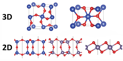
The most familiar 2D material, graphene, is a single layer of carbon, with the same crystal structure as the layers in its 3D counterpart, graphite. By contrast, other materials have stable 2D forms that are structurally distinct from their 3D bulk forms. For example, researchers have recently synthesized 2D with a bi-tetrahedral crystal structure, whereas the 3D form ( quartz) has a trigonal structure. To foresee other 2D group IV oxides, Richard Hennig from the University of Florida, Gainesville, and his colleagues utilized a so-called genetic algorithm that starts off with a random population of candidate structures and then lets them evolve to the most energetically favorable configuration. The results demonstrated that the stable form of 2D should be monoclinic, while 2D and should have a 1T structure. These predicted phases are distinct from the rutile structures found in the 3D versions of these oxides.
Further calculations showed that it should be possible to synthesize these predicted 2D structures on substrates or as free-standing layers. As for applications, 2D and could be promising candidates for the thin “gate oxide” layer that is essential in certain transistors, while might also work as a protective layer in nanoelectronic devices.
This research is published in Physical Review B.
–Michael Schirber
Michael Schirber is a Corresponding Editor for Physics based in Lyon, France.