Toward Skin-Like Electronics
Able to rapidly and simultaneously capture countless signals, skin is one of the most powerful “electronic” systems in the world. With 3000 sensory cells per square centimeter, it provides us with data about temperature, humidity, and pressure in our environment. It is also stretchable, biodegradable, self-healing, and autonomous—it requires no direct input from the person to carry out its tasks.
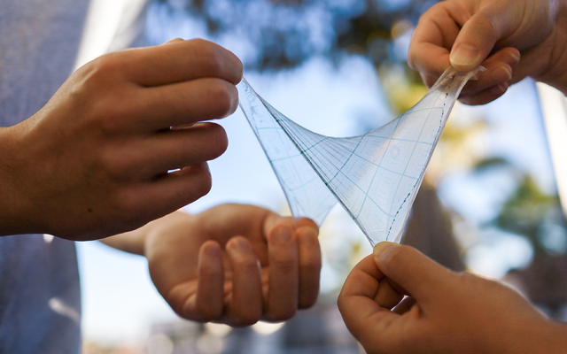
These enviable properties have made creating electronic “skin” a goal of many scientists, including Zhenan Bao of Stanford University, who has been working on the problem for over two decades. At the recent ACS Fall Meeting, Bao presented her latest work on this topic: a method for fabricating high-density arrays of flexible transistors. The method can assemble 42,000 transistors per square centimeter of material, a density over 2 orders of magnitude higher than that achievable through other techniques.
Since its invention in the 1940s, the transistor, which is used to control an electronic signal, has been the dominant component of most electronic systems. Today, transistors are largely made of silicon because of its unparalleled electronic properties. But silicon is a poor fit for making electronic skin, as silicon-based devices are inflexible and brittle—the opposite of human skin.
When Bao started developing electronic skin, high-performing, stretchable electronic materials were nearly nonexistent, so she set about synthesizing polymers that could fill that gap. Today, the polymers that she has made can conduct electrons at speeds exceeding those of amorphous silicon (often used in thin-film electronics). But, for the devices that Bao would like to make—for example, an electronic body suit that would monitor nerve signals throughout the body—there are still hurdles to overcome. One of those is making the high-density sheets of transistors that will be required to simultaneously capture and process all of the body’s electronic signals.
Solving that problem, Bao says, is where her method comes in. “To make stretchable electronic devices, it’s not possible for us to simply swap the silicon with a polymer,” she says. Silicon devices are fabricated at very high temperatures using processes and chemicals that destroy her polymers. “That’s why we have to develop new processes for our materials.”
The method developed by Bao and her colleagues fabricates 2- 𝜇m-wide transistors from semiconducting polymers using ultraviolet light. The first step is to coat a silicon wafer with a water-soluble material and then with a stretchable, inert material, which acts as the base for the “skin.” On top of this base, the researchers deposit a roughly 150-nm-thick layer of a conducting polymer. Rectangular structures are then created in this layer by passing ultraviolet light through a patterned mask. Exposed regions form bonds, or “crosslinks,” between polymers. The crosslinked parts become the gates of a transistor, while unexposed polymer regions are washed away.
The patterning and washing steps are repeated three more times to create the dielectric, semiconducting, and source/drain features of the transistors. The skin is released from the wafer by dissolving the water-soluble layer, revealing the stretchable system.
Bao notes that silicon electronics are also patterned this way, using the same light-and-mask hardware. The choice to replicate that technology was intentional, as it means that facilities that currently make rigid silicon devices could switch to making flexible polymer ones without having to buy new equipment. But, she adds, the hardware is where the similarities end. The patterning processes are different, as the polymer components are directly photopatterned in her technique, while, for silicon, it is done indirectly via additional photoresists. The techniques also use different chemicals for the patterning and are conducted at different temperatures.
For the first demonstration of their technique, the team achieved a density of 42,000 transistors per centimeter, largely surpassing their previous record of 348 polymer-based transistors per square centimeter. That jump is big, but Bao says she would like to make it even bigger—an improvement that would require synthesizing new polymers with better electrical properties.
If the density can be increased, she envisions that her skin electronics might be incorporated into suits or helmets that would allow researchers to monitor signals from the brain or understand how different electrical signals in the human body interact with one another. Bao is also working on incorporating her polymer-based electronics into devices that would go inside the body to directly monitor the signals from the heart or some other organ. “There are endless possibilities for this technology,” she says. “I want to push it as far as I can.”
–Katherine Wright
Katherine Wright is the Deputy Editor of Physics Magazine.


