Spectroscopy That Doesn’t Scratch the Surface
The electronic states of a material’s surface might only be 2D, but they offer a depth of interesting physics. Such states, which are distinct from those of the material’s bulk, dominate many phenomena, such as electrical conduction, magnetism, and catalysis, and they are responsible for nontrivial surface effects found in topological materials and systems with strong spin-orbit interaction. Surface electronic states also control the properties of so-called 2D materials, such as graphene. To understand surface phenomena and harness them in practical devices, researchers chiefly rely on photoemission spectroscopy, which measures the energy and momentum of electrons emitted when photons hit the material. The high resolution with which electron energy and momentum can be characterized allows physicists to measure both the band structure and the density of states (DOS) in the few surface layers where escaping photoelectrons originate. However, the contribution of bulk electrons to photoemission signals makes it difficult to obtain the electronic states of only the outermost layer of a sample. Now Alexander Fairchild at the University of Texas at Arlington (UTA) and colleagues have invented a new method—based on a modification of a technique that liberates electrons using positrons rather than photons—to selectively determine the electron DOS of the first surface layer without any contributions from the bulk [1].
The team’s technique, called Auger-mediated positron surface sticking (AMPS), is not the first that can determine the electronic states of a material’s top-most layer. So far, several such methods have been created, the best known being spectroscopic-imaging scanning tunneling microscopy [2]. In this method, Fourier transformation of the real-space image allows researchers to measure the surface local DOS and to map the electronic states in k-space. A limitation is that the sample must be electrically conductive. A second method for probing surface electronic states is metastable-atom deexcitation spectroscopy, in which the material surface is probed using atoms (typically, helium) that have been excited to a metastable electronic state [3]. These metastable atoms pick up electrons at the first surface layer, which causes the atoms to decay to the ground state. The excess energy liberated through the decay provides the DOS of the first surface layer. A limitation of this technique is the fact that in metals the decay occurs through a so-called Auger process involving two electrons, making it difficult to reconstruct the electronic bands. New methods are required to compensate for the weaknesses of these techniques.
A promising approach is positronium spectroscopy. In this method, a positron beam scanned across the sample implants positrons into the subsurface region. These positrons diffuse back to the surface and, after picking up electrons, they are emitted as positronium, an electron-positron bound state. In the sample’s bulk, the high electron density screens the Coulomb interaction between a positron and an electron, meaning positronium is formed only in the low-electron-density region beyond the material’s outer surface, where the screening effect vanishes. This ensures that the detected positronium particles carry energy and momentum information about electrons in only the first surface layer. Recently, a group at the University of California, Riverside, succeeded in obtaining the DOS of a copper surface by measuring the positronium energy spectrum with meV energy resolution [4], while my own group observed the spin-polarized electronic states of certain ferromagnet surfaces [5]. However, this method is only applicable to systems with a negative positronium work function, that is, systems in which positronium atoms are spontaneously emitted. For example, bismuth-based topological insulators—which are widely used models for research into topological materials—have a positive positronium work function and hence cannot be inspected using positronium spectroscopy. The new AMPS method has no such restriction.
The new method grows out of work conducted by the UTA group to develop magnetically guided, low-energy positron beams for positron annihilation-induced Auger electron spectroscopy, in which positrons projected at the sample form bound states on the sample’s surface [6]. Eventually, these positrons annihilate with core electrons of the surface atoms, leaving core holes. As electrons from higher states make the transition to fill the core holes, the excess energy is emitted via Auger electrons, the energies of which convey information about the surface electronic state. If the width of the valence band is large enough (10–20 eV), then Auger electrons from the valence band are also emitted via the transition of valence electrons into deeper valence holes [7]. (The spectrum of this “VVV” Auger process has long been overlooked in conventional Auger electron spectroscopy.)
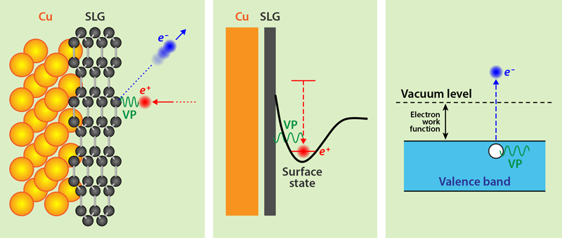
The UTA group discovered an additional Auger electron spectrum—different from both the core-hole-mediated peaks and the VVV spectrum—that emerges when the positron energy exceeds a certain threshold. This spectrum, which AMPS exploits, reflects the contribution of a distinct Auger-emission process in which the positrons don’t penetrate the sample but are captured in the mirror potential formed outside of the surface. Because there is no need for the spontaneous emission of positronium atoms, the technique can be used to characterize materials with a positive positronium work function. And because the positrons interact with surface electrons via “virtual” photons that do not penetrate the sample, the energy spectrum of the Auger electrons emitted via the AMPS process represent the DOS of the outermost surface layer only. The team confirmed the surface specificity of AMPS by applying the technique to a clean copper surface and to a single layer of graphene on a copper substrate (Fig. 1). They found that the AMPS spectrum shape differed significantly for the two surfaces: the spectrum for the clean copper surface showed a broad feature determined by the contribution of the material’s 3d and 4s electrons, while the graphene exhibited the expected “Dirac cone” DOS shape with no contribution from the underlying copper layer.
There are many potential applications for a spectroscopy method that is sensitive to only the surface DOS. While Fairchild and colleagues showed that the pure graphene on copper maintained the characteristic linear dispersion of the Dirac cone, it is predicted that the Dirac cone of graphene on other 3D metals, such as cobalt and nickel, will be destroyed because of better lattice matching between graphene and those metals [8]. A systematic survey of the modulation of graphene’s band structure depending on the substrate material would be important to confirm this prediction [9]. Topological surface states might also be intriguing in a similar context. The energy resolution of the AMPS method is approximately 0.2–0.5 eV for electron energies of 1–5 eV [10]. Improving this resolution will be essential to observe the surface DOS in more detail. Such an improvement will make the observation of an energy gap in some 2D superconductors a realistic prospect, potentially confirming that Cooper pairs exist at a superconductor’s top-most layer. Additionally, if spin-polarized AMPS spectroscopy becomes available, more applications in spintronics can be envisioned.
References
- A. J. Fairchild et al., “Photoemission spectroscopy using virtual photons emitted by positron sticking: A complementary probe for top-layer surface electronic structures,” Phys. Rev. Lett. 129, 106801 (2022).
- S. Edkins, Spectroscopic-imaging STM (SI-STM), in Visualising the Charge and Cooper-Pair Density Waves in Cuprates, Springer Theses. (Springer, Cham. 2017).
- Y. Yamauchi and M. Kurahashi, “Spin-polarized metastable deexcitation spectroscopy study of iron films,” Appl. Surf. Sci. 169-170, 236 (2001).
- A. C. L. Jones et al., “Angle-resolved spectroscopy of positronium emission from a Cu(110) surface,” Phys. Rev. Lett. 117, 216402 (2016).
- M. Maekawa et al., “Spin-polarized positronium time-of-flight spectroscopy for probing spin-polarized surface electronic states,” Phys. Rev. Lett. 126, 186401 (2021).
- A. Weiss et al., “Auger-electron emission resulting from the annihilation of core electrons with low-energy positrons,” Phys. Rev. Lett. 61, 2245 (1988).
- V. A. Chirayath et al., “Auger electron emission initiated by the creation of valence-band holes in graphene by positron annihilation,” Nat. Commun. 8, 16116 (2017).
- A. Miyashita et al., “Spin polarization of graphene and h-BN on Co(001) and Ni(111) observed by spin-polarized surface positronium spectroscopy,” Phys. Rev. B 97, 195405 (2018).
- Y. Fukaya et al., “Spacing between graphene and metal substrates studied with total-reflection high-energy positron diffraction,” Carbon 103, 1 (2016).
- S. Mukherjee et al., “Time of flight spectrometer for background-free positron annihilation induced Auger electron spectroscopy,” Rev. Sci. Instrum. 87, 035114 (2016).