Adapting a Surface Microscopy Tool for Quantum Studies
Often, the best way to understand the structure and behavior of a material is to examine it under a microscope. To reveal features on a scale smaller than the wavelength of visible light—about 1/100th the width of human hair—electrons are often the right tool for the job. Researchers have used transmission electron microscopes (TEMs) to image the motion of single atoms and the structure of SARS-CoV-2, the virus that causes COVID-19. Scanning electron microscopes (SEMs) are smaller and less expensive instruments that operate at lower energies and can image the surface of a material in its original form. SEMs can map the elemental composition of rocks right out of the ground, identify single nanoscale defects in hundreds of thousands of computer chips, and even print 3D microscale prototypes. In addition to their day jobs as imaging tools, TEMs have recently taken up a side hustle as a workbench for quantum-mechanics experiments. Now, researchers from the University of Erlangen-Nuremberg in Germany have built an SEM with quantum credentials [1].
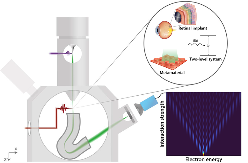
One avenue for quantum experiments in an electron microscope involves simultaneously shooting electrons and a laser beam at a material so that electrons inelastically scatter with the laser photons[2]. Electrons cannot absorb or emit a photon in free space as doing so would violate conservation of energy and momentum. However, a material offers just the kick needed to conserve both energy and momentum so an electron can exchange photons with the laser field [3]. An electron energy spectrum recorded after many electrons have participated in this inelastic electron-light interaction shows a range of evenly spaced peaks separated by the photon energy of the laser (Fig. 1). Because the laser field essentially behaves in a classical way, electrons emerge from the interaction in a controllable, nearly pure quantum state—in other words, the laser can be used to shape the electron state. And the electron state is special: a train of attosecond electron pulses forms with a period equal to the optical cycle of the laser [4]. These pulses could probe the fastest dynamics in materials [4]. A second interaction can then reverse the first one—and restore the original electron state—through destructive interference [5]. Inelastic electron-light scattering (IELS) can prepare electrons into an engineered quantum state for the purposes of imaging or studying quantum interactions.
Between the potential to directly image the fastest material dynamics at atomic scales and the ability to engineer electron states using a laser, excitement has grown recently about IELS. For example, on the basic quantum side, researchers have used IELS to swirl electrons into a vortex state [6]. On the applied side, imaging with IELS is called photon-induced near-field electron microscopy (PINEM). PINEM has imaged the optical properties of systems such as surface plasmons and nanoparticles [2], proteins and cells [7], and even chiral nanostructures [8]. The SEM built by the University of Erlangen-Nuremberg team is capable of both performing quantum-mechanics experiments with electrons and imaging challenging specimens with PINEM.
PINEM was first developed in a TEM, an area where electron spectrometers are commercially available. Measuring the quantized change in electron energy that occurs when electrons interact with the laser field is relatively easy. The tricky part is achieving a high laser field: femtosecond or picosecond electron and laser pulses are typically used for the combination of high peak fields and low average power [3]. For multiple IELS interactions, which are necessary for more elaborate engineering of the electron state, the millimeter-scale gap where specimens sit in a TEM limits the tool’s versatility, whereas SEMs have a large specimen chamber that the operator can reach into with both hands, making experiments with multiple IELS interactions easier. The lower available electron energies of an SEM may also prove useful for a range of specimens; there may be resonances or other maxima in the electron-light scattering depending on geometry [7, 8], or the PINEM signal may be too weak at TEM energies to effectively image the specimen but sufficiently strong at lower energies [3, 8]. Additionally, the lower cost of SEMs makes them more accessible to new groups wanting to do IELS or PINEM experiments.
The instrument that the team developed makes PINEM possible in an SEM. They modified an electron source to produce picosecond electron pulses when struck by a laser pulse, added a path for a femtosecond pulsed laser to excite the specimen, and built an electron spectrometer for their SEM. Each of these steps is a significant project, but the group really triumphed by tying all the elements together: they characterized the instrument and probed a tungsten needle with PINEM. The measured electron spectra matched their simulations remarkably well, which suggests that they have an excellent understanding of the instrument they designed.
It will be exciting to see what experiments follow with this instrument. The ample space in an SEM chamber allowed this group to place a lens with a short focal length very close to the specimen. Doing so may allow them to produce a high laser field on the specimen. The tightly focused laser spot leads to a higher PINEM signal without increasing the average temperature of the specimen, making specimens with a weaker optical response more practical to image. PINEM in an SEM could also shed new light on larger specimens, such as a 3D metamaterial device, that do not fit into a TEM. This new microscope may help motivate the increasing availability of commercial SEM electron spectrometers, which would make building future PINEM-SEMs far easier. The wide-open specimen chamber and the uniquely low energy range give this instrument the ability to push the limits of PINEM imaging and of quantum experiments with electrons.
References
- R. Shiloh et al., “Quantum-coherent light-electron interaction in a scanning electron microscope,” Phys. Rev. Lett. 128, 235301 (2022).
- B. Barwick et al., “Photon-induced near-field electron microscopy,” Nature 462, 902 (2009).
- S. T. Park et al., “Photon-induced near-field electron microscopy (PINEM): theoretical and experimental,” New J. Phys. 12, 123028 (2010).
- K. E. Priebe et al., “Attosecond electron pulse trains and quantum state reconstruction in ultrafast transmission electron microscopy,” Nat. Photon. 11, 793 (2017).
- K. E. Echternkamp et al., “Ramsey-type phase control of free-electron beams,” Nat. Phys. 12, 1000 (2016).
- G. M. Vanacore et al., “Ultrafast generation and control of an electron vortex beam via chiral plasmonic near fields,” Nat. Mater. 18, 573 (2019).
- T. R. Harvey et al., “Probing chirality with inelastic electron-light scattering,” Nano Lett. 20, 4377 (2020).
- N. Talebi, “Strong interaction of slow electrons with near-field light visited from first principles,” Phys. Rev. Lett. 125, 080401 (2020).