Proper carbon ID required
The ability to image surfaces with atomic-scale resolution in the 1980s ushered in the nanotechnology era. From the beginning, it was understood that although scanning tunneling microscopy (STM) could resolve distances between individual atoms on surfaces, what the images really showed were spatial variations in the electronic density of states of the surface near the Fermi level [1]. Since the density of states does not always peak when the tip is directly above the atoms, microscopists have always been left asking the question: What does one see in “atomic-resolution” STM images? The more recent development of atomic-resolution noncontact atomic force microscopy (NC-AFM) promised to alleviate this uncertainty [2]. In NC-AFM, the contrast is due to variations in the attractive force between the surface and the end of the tip, an interaction expected to be strongest directly above the surface atoms. Experiments quickly showed, however, that images of the same surface could appear completely different depending on the structure and composition of the end of the AFM tip [3]; therefore, interpreting these images required an understanding of the short-range chemical forces acting between the surface and the possible species at the end of the tip. The issue of what we actually see in atomic-scale images has been particularly vexing for materials constructed from graphene sheets. In a paper appearing in Physical Review Letters, Martin Ondráček, of the Academy of Sciences in the Czech Republic, and colleagues [4] show theoretically how changing the tip changes the answer to the simple question: Are we imaging atoms? and guides experimentalists as to how they should prepare tips for stable, high-resolution imaging.
The basal ( ) plane of graphite was a favorite early test system for scanning probe microscopy, as much for intrinsic interest in the material as for the ease with which extremely well-ordered, chemically inert surfaces that remain clean for days in air could be created. It is also a prime example of STM images not reflecting the positions of the atoms on the surface: Although the carbon atoms on the graphite basal plane are arranged in a honeycomb pattern with two atoms per unit cell, STM images show hexagonal symmetry with one feature per unit cell. This difference could be explained by the way carbon sheets are stacked in graphene: Half the atoms on a graphite surface lie directly above a carbon atom in the sheet one layer down. These carbon atoms have a lower density of states compared to their neighbors that lie on top of a hollow site [5]. The result is that STM only sees every other carbon atom on the surface. Meanwhile, NC-AFM images also generally show only one feature per unit cell [6].These findings would have faded from the spotlight if not for the intense interest in nanostructures constructed by rolling up, twisting, and isolating the graphene layers that make up graphite [7]. As the properties of these new forms of carbon depend sensitively on their local structures and defects, characterizing these materials on the atomic scale is essential to progress in understanding and exploiting their unique properties. Thus we are again left asking, what do we see in STM and NC-AFM images of carbon nanostructures? Ondráček and co-workers have stepped into this breech.
Ondráček et al. address contrast mechanisms in NC-AFM through a hybrid theoretical approach. They model the short-range interactions between the atoms at the very end of the tip and the surface, using density-functional theory (DFT), and estimate the long range van der Waal’s type forces between the entire tip shank and the surface with a semiempirical potential. They show that even for inert tips and surfaces where the van der Waal’s interaction dominates the total tip-surface interaction, both long- and short-ranged interactions must be included to understand the contrast mechanism. For currents in STM, the group’s approach is to consider the tip and sample as a single system with a rigorous description of tunneling that includes multiple scattering effects; these details are needed to accurately model the current when the tip is very close to the surface [8].
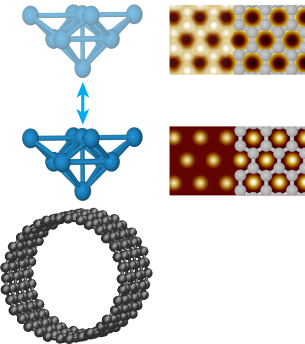
Ondráček et al. consider surfaces of a single-walled carbon nanotube (SWCNT) and a graphene bilayer with inert tips and reactive tips. The inert tips terminate in closed-shell electronic configurations. With such tips, the hollows are predicted to appear bright in NC-AFM images of SWCNT, consistent with the hexagonal symmetry most often seen experimentally (Fig. 1). As a SWCNT contains only a single graphene sheet, the hexagonal symmetry must reflect a stronger interaction with the hollow site. This had been interpreted purely in terms of van der Waals interactions that could be maximized at the hollow through interaction with the six neighboring carbon atoms simultaneously [6]. The situation is actually more complex. In the attractive regime, Ondráček et al. see essentially no difference between both the short- and long-range interactions when the tip is positioned above a hollow site or an occupied site. The short-range interaction, however, becomes repulsive above the carbon atoms before it does so above the hollow sites; meanwhile the long-range interaction remains attractive. When the forces due to these interactions are summed, the repulsion of the short-range interaction at the on-top site decreases the total force between the tip and sample compared to the hollow site, while still in the overall attractive regime. Thus it is the short-range Pauli repulsion between the closed shell electron clouds of the tip and sample that cause the hollow site to appear bright, not the van der Waals interaction. Although not responsible for the contrast, the long-range interaction remains larger and sets the total magnitude of the interaction and enables contrast, while still in the overall attractive regime. Thus, even for inert tips and samples, both short- and long-range interactions must be considered.
Not surprisingly, the situation changes for reactive tips. For tips terminating in Si dangling bonds, an interaction akin to a chemical bond can occur when the tip is positioned above a carbon atom but not a hollow site, and so now the carbon atoms appear bright in NC-AFM images. Tungsten tips are found to be less chemically specific—they experience chemical bonding interactions at the on-top and hollow sites of both SWCNT and bilayer graphene. These attractive interactions, however, maximize at different distances from the surface, further away for the on-top site. As a result, the contrast is predicted to change from honeycomb to hexagonal as the tungsten tip nears the surface, as illustrated in Fig. 1. Interestingly, the contrast in STM images may also change when the tip gets very close to the graphene bilayer surface. As the tip-sample separation is reduced below , Ondráček et al. predict a transition from the usual contrast, where only half the carbon atoms are visible, to the hollows appearing bright as the current above the carbon atoms saturates; a transition that may also occur for close-packed metal surfaces. Although both give identical hexagonal symmetry, this result has implications for combined STM/NC-AFM imaging. Mainly, the positions of the bright spots in a single STM image of even a well-understood surface cannot be used to establish the atomic registry of the NC-AFM data.
The answer “it depends” to the question “are we seeing atoms?” may seem unsatisfying at first. Fortunately, in the last few years there has been a great progression from recording individual STM or NC-AFM images with unknown tips, to obtaining the data necessary to assign atomic-scale features to specific surface sites. This means having the ability to place specific molecules at the end of the tip [9] and to fully map the evolution of currents and forces as the tip moves toward the surface with resolution and across the surface with resolution [10]. Ondráček et al. offer a pathway to exploit the former to stably and reproducibly image molecules and nanostructures constructed from aromatic rings. Specifically, attaching a closed-shell molecule to the end of the tip consistently emphasizes the centers of a ring of carbon atoms in NC-AFM images, while other species emphasize other chemical groups [9]. Meanwhile, atomic-scale mapping of tunneling currents and forces as a function of distance from the carbon nanostructure surface with metallic tips offers the promise of imaging all of the surface sites in a single experiment. Such data is essential to detect defects that would either not be detected or would not be possible to assign to specific atomic structures through typical unit-cell resolution images. Beyond carbon nanostructures, Ondráček et al.’s results demonstrate that theory and computational methods and hardware have advanced to the point where it is possible to accurately model the electronic, chemical, and physical interactions responsible for contrast in scanning probe microscopy (SPM). Thus the theoretical and experimental tools are now coming into place to start a new era in SPM in which all of the atoms on a surface can be identified and their chemical and electronic properties characterized [11,12]. In this new era, theory’s role will shift from explanation to design of stable, atomic-resolution tips, optimized to interrogate specific chemical, electronic, or physical interactions.
References
- J. Tersoff and D. R. Hamann, Phys. Rev. Lett. 50, 1998 (1983)
- F. J. Giessibl, Science 267, 68 (1995)
- J. V. Lauritsen et al., Nanotechnology 17, 3436 (2006)
- M. Ondráček, P. Pou, V. Rozsíval, C. González, P. Jelínek, and R. Pérez, Phys. Rev. Lett. 106, 176101 (2011)
- I. P. Batra, N. García, H. Rohrer, H. Salemink, E. Stoll, and S. Ciraci, Surf. Sci. 181, 126 (1987)
- H. Hölscher, W. Allers, U. D. Schwarz, A. Schwarz, and R. Wiesendanger, Phys. Rev. B 62, 6967 (2000)
- A. K. Geim and K. S. Novoselov, Nature Mater 6, 183 (2007)
- J. M. Blanco et al., Phys. Rev. B 70, 085405 (2004)
- L. Gross, F. Mohn, N. Moll, P. Liljeroth, and G. Meyer, Science 325, 1110 (2009)
- B. J. Albers, T. C. Schwendemann, M. Z. Baykara, N. Pilet, M. Liebmann, E. I. Altman, and U. D. Schwarz, Nature Nanotech. 4, 307 (2009)
- M. Z. Baykara, T. C. Schwendemann, E. I. Altman, and U. D. Schwarz, Adv. Mater. 22, 2838 (2010)
- Y. Sugimoto, P. Pou, M. Abe, P. Jelinek, R. Perez, S. Morita, and O. Custance, Nature 446, 64 (2007)