Cutting Losses for Surface Light
Light propagating in concert with electrons along a metal surface may one day be used to turn microchips into optical processors. Researchers report in Physical Review Letters that the loss of energy suffered by such metal-skimming light waves can be reduced if the waves are produced at a nanoscale slit in the metal film that carries the waves. The measurements are the first to provide a direct probe of the light losses in the vicinity of a subwavelength aperture. The authors explain the effect as the result of interference between two different kinds of waves generated by the slit.
Researchers are currently developing materials that can produce and manipulate hybrid light-electron waves called surface plasmon polaritons (SPPs or simply “plasmons”). These devices have the potential to transport optical information along nanometer-thick metal wires. However, electron collisions in the metal rob the SPPs of energy that instead goes into heating the material.
Some researchers are looking for an amplification medium that could compensate for these losses, but Philippe Lalanne from the University of Bordeaux in France and his colleagues have perhaps found another way using so-called subwavelength apertures. As shown 16 years ago [1], holes or slits etched in a metal film can generate SPPs when illuminated by light whose wavelength is greater than the aperture size. Current efforts are focused on developing these apertures as “plasmon launchers,” but little research has been done so far on the losses that occur near the holes or slits, Lalanne says
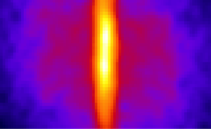
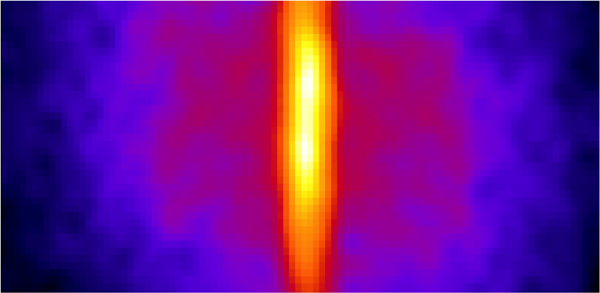
Lalanne and his team created a 300-nanometer-wide slit in a gold film deposited on a glass substrate. They illuminated the film from below with an infrared ( 800 nanometer) laser pulse, producing SPPs on the top surface, propagating outward, perpendicular to the slit direction. As the waves died out and were absorbed by the metal, they heated it enough to affect the surface’s ability to reflect light. So the team probed the SPP absorption by firing a second, time-delayed laser ( 532 nanometers) at many locations on the top of the film and detected the reflected light. These so-called thermoreflectance data showed a plateau between 5 and 15 micrometers from the slit, which meant that the absorption was constant over this region.
The constant absorption came as a surprise. The absorption is proportional to the SPP intensity, so one would expect it to decrease with distance from the slit source. The researchers say wave interference is responsible for the anomaly. In previous work, Lalanne and his collaborators had shown that subwavelength slits produce not only SPPs, but also another type of light, which they called quasicylindrical waves (QCWs) [2]. QCWs propagate in all directions above the film with nearly cylindrical wave fronts and with a wavelength almost equal to that of the SPPs. In new calculations, the team shows that the QCWs destructively interfere with the SPPs, and with a diminished SPP intensity, there is less for the gold to absorb. The interference effect is strongest closer to the slit and fades away by about 15 micrometers, as the QCW intensity decreases relative to the SPPs. This pattern of interference explains the thermoreflectance plateau and should produce plateaus for other slit or hole geometries, according to the team’s calculations.
Constructive interference also occurs between the QCWs and SPPs, causing increased absorption close to the slit opening, and the total absorption by the metal turns out to be about the same as it would have been without the QCWs. “But we also show that one can engineer a system to lower the total absorption,” Lalanne says. To do that, they imagine placing a silicon nanowire just above the slit, which changes the phase between the QCWs and the SPPs. If the light only needs to propagate a few micrometers as part of a future optical circuit, then the loss to absorption can be reduced by 10 to 50 percent, the team calculates.
“It’s an intriguing result,” says Martin van Exter of Leiden University in the Netherlands. He says that reducing the need for gain could help in the development of an SPP laser. Kobus Kuipers of the Foundation for Fundamental Research on Matter Institute for Atomic and Molecular Physics (AMOLF) in Amsterdam is surprised by the findings, but he believes the authors provide a convincing argument to explain the absorption. “I am certain that this result will be picked up by many and that it will spark a flurry of exciting optical physics activity at the nanoscale,” Kuipers says.
–Michael Schirber
Michael Schirber is a Corresponding Editor for Physics Magazine based in Lyon, France.
References
- T. W. Ebbesen, H. J. Lezec, H. F. Ghaemi, T. Thio, and P. A. Wolff, “Extraordinary Optical Transmission through Sub-Wavelength Hole Arrays,” Nature 391, 667 (1998)
- P. Lalanne, J .P. Hugonin, H. T. Liu, and B. Wang, “A Microscopic View of the Electromagnetic Properties of Sub-λ Metallic Surfaces,” Surf. Sci. Rep. 64, 453 (2009)


