Tracking Electron Movements in Bilayer Graphene
Graphene—the one-atom-thick layer of pure carbon discovered in 2004—attracts strong interest for industrial applications because of its high mobility, optical transparency, flexibility, mechanical robustness, and environmental stability. The rapid progress in the fabrication and manipulation of graphene layers motivates its integration into electronic devices [1] that, in principle, could be much smaller than their silicon counterparts. However, a key obstacle blocks the development of graphene-based circuits: graphene is not currently suitable for transistors—the essential building blocks of modern electronics. For a field effect transistor (FET) to be technologically viable, only a small electric current must flow through its gate in the stand-by state, to ensure low power consumption. But graphene does not have an electronic band gap and therefore always conducts current: Graphene FETs cannot switch off. On the contrary, the switch-off ability of silicon FETs is one of the key reasons why silicon logic circuits have bested all competing technologies.
How could the switch-off performance of graphene-based FETs be improved? Recently, a new material consisting of two layers of graphene (bilayer graphene) seemed to offer a possible solution: while the material is gapless, an applied electric field can create a band gap. But a number of experiments showed that biased bilayer graphene does not behave exactly as a semiconductor, and the FETs so far realized with this material do not feature satisfactory performances. Reporting in Physical Review Letters [2], a research team led by Philip Hofmann at the Aarhus University, Denmark, has now shed light on bilayer graphene’s electronic behavior. The researchers monitored the movement of electrons in bilayer graphene in real time using an advanced form of time-resolved photoelectron spectroscopy. The results confirm that the description of the material as having a semiconducting band gap is appropriate, and may suggest material growth strategies leading to better bilayer-graphene FETs.
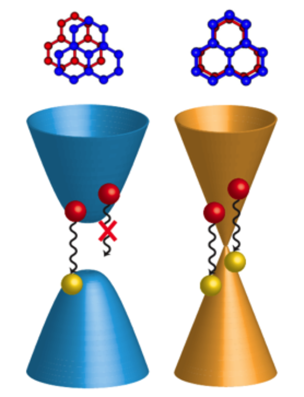
Bilayer graphene consists of two layers of graphene with “ stacking” (the atoms of the second graphene layer sit at the center of the honeycomb lattice’s hexagons of the first layer). In isolation, such a system is still gapless. However, theorists have predicted that any external perturbation, such as the application of an electric field or the placement of the bilayer on a substrate, would make the two layers inequivalent and alter the band structure [3]. Recent experiments have revealed that an applied electric field, perpendicular to the bilayer’s plane, creates an electronic gap, turning the material into a semiconductor [4], with a band gap of up to – milli-electron-volts for applied voltages of a few volts. Bilayer graphene has indeed been used to fabricate FETs whose carrier mobility is comparable to that of bulk silicon. But the reported on-off current ratio ( at room temperature and at low temperature [5]), while order of magnitude better than the single layer’s, is still too small for logic applications (silicon FETs’ values range between and ). Apparently, in spite of its band gap, bilayer graphene does not behave as a small-gap semiconductor but rather as a sort of semimetal—a material in which there is a small overlap between conduction and valence band (i.e., it is gapless), but with much fewer conducting carriers than a metal. The gap may be closed by material imperfections, which generate midgap electronic states where electrons can efficiently tunnel, generating a steady metallic conduction that limits the switching ratio.
There is a possible explanation for the formation of such midgap states: the emergence, due to structural distortions or strain, of small twists—an imperfection sufficient to generate patches with stacking instead of . Since bilayers are gapless, these patches would offer possible conductive paths in the solid. Previous static angle-resolved photoemission spectroscopy (ARPES)—the most direct method for studying the electronic structure of the surface of solids—has indeed indicated the presence of electronic states dispersed throughout the gap and suggested they are consistent with the presence of twisted domains [6]. Alternatively, a strain-induced network of dislocations (walls dividing domains with different stacking) [7] may also lead to a measurable density of midgap states. But how do these states affect electron transport? Do they short circuit the electron dynamics throughout the sample (turning it into a semimetal)? Or do they lead to isolated and local changes of the electronic structure, and do charge carriers still feel a band gap while moving in the -stacked domains (i.e., it is a semiconductor with local conductive paths)?
To address such a key question, Philip Hofmann and his co-workers have collected snapshots of electrons moving in the valence and conduction bands of bilayer graphene, applying time- and angle-resolved photoelectron spectroscopy (TR-ARPES)—a natural extension of conventional ARPES. TR-ARPES is able to probe all the observables accessed by ARPES as a function of time, with a resolution that can reach the -femtosecond ( ) regime. Its working principle is common to all pump-probe detection schemes: An intense infrared pump pulse hits the sample, inducing direct electronic transitions between valence and conduction bands. This creates a population of photoexcited electrons in the conduction band, which then relax. A second fraction of the laser output generates a synchronized femtosecond beam in the uv or soft x-ray range. This probing pulse causes the material to emit electrons after a variable delay from the arrival of the pump pulse. By measuring the energy and momentum of these photoemitted electrons as a function of time, the method delivers a sequence of snapshots of the direction, speed, and scattering mechanisms of electrons inside the sample. Since in graphene the structure of the electronic states and the lattice are only weakly affected by the near-infrared pumping used by the authors, the setup basically measured the transient occupation factor of the relevant electronic bands (conduction and valence).
The results provided a detailed picture of the different steps by which carriers relax (see Fig 1). First, the photoexcited electrons (holes) cascade down to the bottom of the conduction band (top of the valence band). This relaxation process, which lasts – , is driven by impact ionization (electrons losing energy by knocking out other electrons from the valence band) and by the displacement of the positions of atoms in the lattice (through the emission of so-called optical phonons). This leads to a transient state in the form of an electron-hole plasma [8,9] and by a nonequilibrium distribution of optical phonons [10]. Afterwards, the excited electrons reduce their excess energy below the threshold for optical phonon emission and relax from valence to conduction band by emission of acoustic phonons. This longer-term dynamics takes place on the picosecond timescale and is most sensitive to the presence of a gap because electrons and holes must release a quantum of energy comparable to the gap size in order to recombine. If the gap is larger than the quantum energy of the available phonons, the electron-hole recombination is hindered by energy conservation: an electron and a hole cannot recombine and lose their energy through the emission of one phonon. Relaxation then has to rely on multiphonon processes, radiative emission, or the recombination via midgap states.
Among these mechanisms, only the last one could be fast enough to neutralize the effect of an ideal band gap on the dynamics. If midgap states act as effective tunneling channels for recombination, the process can be as fast as in single-layer graphene. But here comes the key finding by Hofmann and colleagues: the recovery to equilibrium conditions is roughly times slower in the case of bilayer graphene than in the single layer sample. This suggests that recombination channels opened by the midgap states are not efficient enough to fully short circuit the electronic motion.
The finding indicates that in bilayer graphene, electrons move as in a semiconductor, albeit under the influence of the midgap states. Future spectroscopic measurements with nanoscale spatial resolution will be key to determine unambiguously if such states are due to stacking imperfections leading to domains and/or to networks of dislocations. But the results of Hofmann and colleagues already suggest that further technological effort should be directed at the minimization of imperfections, for instance, through growth techniques that prevent the formation of domains and minimize the stress-induced dislocations. Once this is done, there is a chance that the switch-off performance of bilayer graphene might be boosted to values sufficient to challenge silicon-based devices.
References
- F. Schwierz, “Graphene transistors,” Nature Nanotech. 5, 487 (2010)
- Søren Ulstrup et al., “Ultrafast Dynamics of Massive Dirac Fermions in Bilayer Graphene,” Phys. Rev. Lett. 112, 257401 (2014)
- E. McCann, “Asymmetry Gap in the Electronic Band Structure of Bilayer Graphene,” Phys. Rev. B 74, 161403 (2006)
- Y. Zhang, T.-T. Tang, C. Girit, Z. Hao, M. C. Martin, A. Zettl, M. F. Crommie, Y. R. Shen, and F. Wang, “Direct Observation of a Widely Tunable Bandgap in Bilayer Graphene,” Nature 459, 820 (2009); E. V. Castro, K. S. Novoselov, S.V. Morozov, N. M. R. Peres, J. M. B. Lopes dos Santos, J. Nilsson, F. Guinea, A. K. Geim, and A. H. Castro Neto, “Biased Bilayer Graphene: Semiconductor with a Gap Tunable by the Electric Field Effect,” Phys. Rev. Lett. 99, 216802 (2007)
- F. Xia, D. B. Farmer, Y.-M. Lin, and Ph. Avouris, “Graphene Field-Effect Transistors with High On/Off Current Ratio and Large Transport Band Gap at Room Temperature,” Nano Lett. 10, 715 (2010)
- K. S. Kim, A. L.Walter, L. Moreschini, T. Seyller, K. Horn, E. Rotenberg, and A. Bostwick, “Coexisting Massive and Massless Dirac Fermions in Symmetry-Broken Bilayer Graphene,” Nature Mater. 12, 887 (2013)
- B. Butz, C. Dolle, F. Niekiel, K. Weber, D. Waldmann, H. B. Weber, B. Meyer, and E. Spiecker, “Dislocations in Bilayer Graphene,” Nature 505, 533 (2014)
- T. Kampfrath, L. Perfetti, F. Schapper, C. Frischkorn, and M. Wolf, “Strongly Coupled Optical Phonons in the Ultrafast Dynamics of the Electronic Energy and Current Relaxation in Graphite,” Phys. Rev. Lett. 95, 187403 (2005)
- T. Limmer, J. Feldmann, and E. Da Como, “Carrier Lifetime in Exfoliated Few-Layer Graphene Determined from Intersubband Optical Transitions,” Phys. Rev. Lett. 110, 217406 (2013)
- H. Yan, D. Song, K. F. Mak, I. Chatzakis, J. Maultzsch, and T. F. Heinz, “Time-Resolved Raman Spectroscopy of Optical Phonons in Graphite: Phonon Anharmonic Coupling and Anomalous Stiffening,” Phys. Rev. B 80, 121403 (2009)