Precise Layering of Organic Semiconductors
The long-standing interest in organic semiconductors (OSCs) is based on the enormous palette of molecules that organic chemistry offers researchers to play with. These organic molecules can be inexpensively processed without the complexity of semiconductor foundries. Electronic devices based on OSCs should have novel properties that would be of basic scientific interest as well as practical significance. Small-molecule OSCs, like pentacene, form weakly bonded (van der Waals) molecular crystals, with comparatively narrow (in energy) conduction and valence bands built from molecular orbitals. This band structure leads to small bandwidths, large effective masses for charge carriers, and low dielectric polarizability compared to traditional inorganic semiconductors. These properties make OSCs attractive for strong correlation physics and other applications, but up until now the highest quality transport and photophysics properties have been observed only in bulk single crystals. In principle, it should be possible to produce bulk-like single-crystal electronic properties with only a few molecular layers, but realizing this possibility has been difficult because of the fragility of OSCs and the challenge of precisely controlling molecular stacking. Yuhan Zhang from Nanjing University, China, and colleagues have achieved this goal, fabricating an OSC field-effect transistor based on epitaxial layer-by-layer growth [1]. Their characterization of the resulting 2D crystalline structures reveals how molecular packing affects the OSC’s electronic properties.
As in inorganic crystals, material purity and structural quality are essential when trying to understand the underlying physics and discern the intrinsic properties of OSC crystals. While comparatively high charge mobilities were demonstrated in bulk organic crystals thirty years ago [2], very often in device structures, the electronic properties of these materials are limited by extrinsic factors arising from the fabrication process. Field-effect transistor (FET) structures exemplify this. FETs are voltage-activated switches with a range of device applications, but they are also excellent tools for physics investigations, since the field effect enables the electrostatic tuning of carrier density without altering the structure of the material. In a typical organic FET, metal source and drain electrodes contact an organic semiconductor channel, and a gate electrode capacitively modulates the charge density in the channel. Organic FET properties can, unfortunately, be strongly affected by difficult-to-characterize extrinsic factors, including chemical impurities, charge trapping at the OSC/dielectric interface, and structural problems like grain boundaries and stacking faults. This can lead to enormous extrinsic variability in measured properties [3] even in nominally identical devices.
Over the last decade, great progress in learning about the intrinsic properties of these materials has been made using FETs and related structures based on bulk single crystals [4, 5]. Vapor-phase transport can produce large, plate-like crystals of a number of small molecule OSCs [6]. Gentle techniques designed to minimize structural damage have led to field-effect measurements that show intrinsic transport properties, e.g., “band-like” conduction with mobility that increases as temperature decreases, higher mobility along particular molecular stacking directions [7], and remarkable effects like the formation of metallic states at heterointerfaces between manually assembled crystals [8, 9]. As promising as these results are in demonstrating high material quality and interesting transport physics, working with bulk single crystals makes practical device configurations difficult.
In order to create scalable devices for applications, reliable thin-film OSCs are needed. However, thin-film growth often results in much higher structural disorder, which does not give the same electronic properties as bulk crystals. For their organic FETs, Zhang et al. grew pentacene films layer-by-layer on atomically flat hexagonal boron nitride (hBN) layers [1]. This epitaxial method takes advantage of the van der Waals forces between the hBN layers and the planar, conjugated molecular structure of the pentacene.
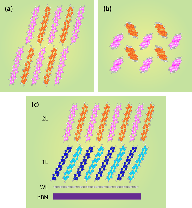
Crucially, Zhang et al. combine this van der Waals epitaxy with multiple complementary characterization techniques: high-resolution atomic force microscopy, selected area electron diffraction via transmission electron microscope, and spatially resolved, polarization-dependent Raman and photoluminescence spectroscopy. The results from these characterization studies verify the structural perfection and purity of the OSC thin films and identify the packing of their constituent molecules. Structurally, Zhang et al. find that the initial wetting monolayer of pentacene lies flat on the hBN. The next layer, termed 1L by the authors, is arranged in a not-previously-reported distortion of herringbone stacking, in which the molecules are flattened along the growth direction (see Fig. 1). The next (2L) and subsequent layers are structurally consistent with the herringbone phase common in pentacene thin films.
The team then compared this detailed structural characterization with electronic transport measurements. To fabricate transistors without ruining the fragile, few-layer epitaxial OSC films, the authors avoided common lithography techniques. Instead, they fabricated gold source/drain electrodes by peeling them from a separate patterned substrate and then mechanically placed these premade electrodes on the OSC layered structure. This novel approach enabled transport measurements down to the single-layer limit in structurally characterized films. The authors found that the flat-lying wetting layer was insulating. By contrast, the 1L structures supported moderate field-effect mobilities of ∼0.1cm2∕Vs at room temperature, which is low compared to silicon’s electron mobility ( 1400cm2∕Vs) but is not unusual for OSC thin-film devices. This mobility increased with temperature. The 2L and thicker structures supported much higher mobilities of ∼3cm2∕Vs at room temperature, with more “band-like” transport. As in bulk single crystals, the 2L layer’s mobility improved upon cooling over a moderate temperature range, particularly at high negative gate voltages.
The observed structures and trends in conduction properties were consistent with density-functional calculations that Zhang et al. performed. These calculations, which model the transport mechanism for conducting hole states, showed explicitly that very high-quality transport can be achieved in ultrathin films, provided that structural disorder is minimized.
While these fragile, few-layer epitaxial OSC devices are not ready for mass production and applications, this work gives insights into how molecular packing is tied to transport. It also points to van der Waals epitaxy as a possible route for achieving bulk, single-crystal-like properties in thin-film devices. Researchers are making great strides growing layered 2D materials with large-area chemical vapor deposition, suggesting that substrates other than mechanically exfoliated hBN could be employed as templates for OSC growth. Moreover, in the course of Zhang et al.’s characterization, they found that the new epitaxial pentacene appears to have excellent optical properties, with bright, clear photoluminescence. Optoelectronic devices based on epitaxial OSCs are therefore promising. The possibilities are manifold for thin-film OSCs, making this growth advance very exciting both scientifically and technologically.
This research is published in Physical Review Letters.
References
- Y. Zhang et al., “Probing Carrier Transport and Structure-Property Relationship of Highly Ordered Organic Semiconductors at the Two-Dimensional Limit,” Phys. Rev. Lett. 116, 016602 (2016).
- W. Warta and N. Karl, “Hot Holes in Naphthalene: High, Electric-Field-Dependent Mobilities,” Phys. Rev. B 32, 1172 (1985).
- S. F. Nelson, Y.-Y. Lin, D. J. Gundlach, and T. N. Jackson, “Temperature-Independent Transport in High-Mobility Pentacene Transistors,” Appl. Phys. Lett. 72, 1854 (1998).
- R. W. I. de Boer, M. E. Gershenson, A. F. Morpurgo, and V. Podzorov, “Organic Single-Crystal Field-Effect Transistors,” Phys. Status Solidi (a) 201, 1302 (2004).
- M. E. Gershenson, V. Podzorov, and A. F. Morpurgo, “Colloquium : Electronic Transport in Single-Crystal Organic Transistors,” Rev. Mod. Phys. 78, 973 (2006).
- H. Jiang and C. Kloc, “Single-Crystal Growth of Organic Semiconductors,” MRS Bulletin 38, 28 (2013).
- V. C. Sundar, J. Zaumseil, V. Podzorov, E. Menard, R. L. Willett, T. Someya, M. E. Gershenson, and J. A. Rogers, “Elastomeric Transistor Stamps: Reversible Probing of Charge Transport in Organic Crystals,” Science 303, 1644 (2004).
- H. Alves, A. S. Molinari, H. Xie, and A. F. Morpurgo, “Metallic Conduction at Organic Charge-Transfer Interfaces,” Nature Mater. 7, 574 (2008).
- I. G. Lezama, M. Nakano, N. A. Minder, Z. Chen, F. V. Di Girolamo, A. Facchetti, and A. F. Morpurgo, “Single-Crystal Organic Charge-Transfer Interfaces Probed using Schottky-Gated Heterostructures,” Nature Mater. 11, 788 (2012).