Current Under a Microscope
As silicon chips shrink ever smaller, understanding their operation at the atomic scale becomes more important. In the 12 January Physical Review Letters, researchers describe an imaging technique that directly reveals, with nanoscale resolution, how current-carrying charges move in semiconductor crystals. Although the first results agree with standard theory, the method should prove useful as chip designers move to still smaller devices, with less easily predictable behavior.
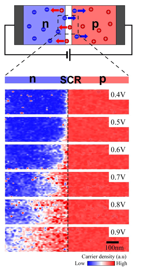
In a so-called n-type semiconductor, an added impurity, or dopant, increases the number of free-moving electrons that can carry current. In a p-type material, a different dopant causes a few electrons to pop out of crowded electron populations in the crystal structure, leaving behind positively-charged “holes” that act as current carriers. When an n-type and a p-type semiconductor are placed in contact, electrons and holes near the boundary diffuse into the opposite material, neutralizing each other and creating a so-called depletion zone that acts as an insulating barrier. Applying a voltage of the correct sign across this p- n junction lessens the barrier, allowing current to flow. This simple device–a diode–is the basic element in transistors and other electronic components.
The standard theory describing how far electrons and holes diffuse in a p- n junction, depending on the voltage, is based on measurements of the total current in the circuit, not on direct observations of the charges themselves. To see if a junction’s microscopic behavior agrees with this theory, Hidemi Shigekawa of the University of Tsukuba in Japan and his colleagues combined scanning tunneling microscopy (STM) with laser illumination to map out the presence of charge carriers. Previous studies combined light with STM to probe semiconductor properties, but none have gotten a direct picture of the carrier density. And none have looked at the semiconductor while current flowed through it.
In STM, the current flowing through a sharp tip just above a surface measures electric fields due to individual atoms. Although STM can pick out dopant atoms in a semiconductor, it cannot accurately measure the charge carrier density because electrons or holes tend to collect near the tip.
A pulse of laser illumination releases additional electrons and holes from the crystal. These extra charge carriers allowed the team to probe the surface in a new way and work out the charge carrier density that would exist without the tip. For example, if charge carriers were already abundant, adding more would have little effect. By contrast, a large change in STM current would indicate a relative scarcity of charge carriers before the laser was turned on. Tip-induced carrier movement “was a big problem for the STM measurement on semiconductors,” says Shigekawa. “But we made the disadvantage into an advantage.”
The researchers mapped the carrier density in a gallium arsenide p- n junction at a resolution of 10 nanometers and confirmed their theoretical predictions: As voltage increased from 0.5 to 0.9 volts, holes migrated on average from 181 to 429 nanometers into the n-side.
“There’s no major surprises here,” says Andreas Heinrich of IBM Almaden Research Center in San Jose, California. “But the fact that they are actually imaging the electric properties is a big step forward.” Surprises may show up when devices shrink below around 50 nanometers, Heinrich says, because dopant atoms will be so scarce that their individual positions may affect the device’s function. Tomihiro Hashizume of Hitachi’s Advanced Research Laboratory in Hatoyama, Japan, says the ability to see precisely how charge carriers move “will be indispensable for the further progress of device miniaturization.”
–Michael Schirber
Michael Schirber is a Corresponding Editor for Physics Magazine based in Lyon, France.