Corrosion Makes Precision Cuts in Silicon
Add a small quantity of the right chemical to a material being squeezed or stretched, and the results can be dramatic. If the chemical reaction is rust, it can trigger cracks that cause a bridge to collapse, but a similar process can lead to precision cuts in silicon, according to the 13 August Physical Review Letters. A team of researchers from several institutions in Europe ran a combination of classical and quantum mechanical computer simulations of a silicon crystal and found that so-called stress-corrosion cracking lies behind a recently developed technique for cutting thin slices of semiconductor for transistors. The atomic-scale study of the process may also help engineers improve the durability of a variety of materials.
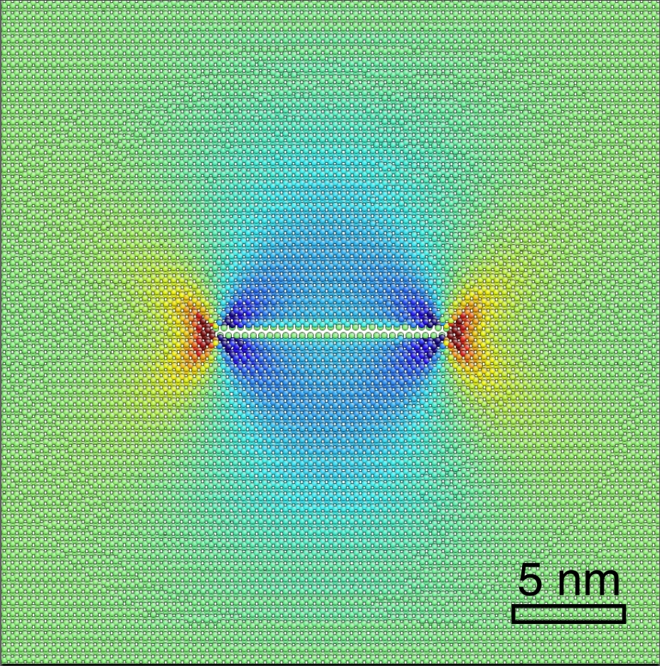
A technique called “Smart Cut” is used to electrically insulate a very thin layer of silicon from another, thicker layer. The critical part of the process involves shooting a beam of hydrogen ions into the wafer, so that they are implanted and form a thin layer a few tens of nanometers below the surface. Heating the wafer generates nanometer-scale, disk-shaped regions of broken silicon bonds, or defects, in the hydrogen layer, and these regions grow, join together, and eventually slice the silicon.
To date, in the absence of a detailed understanding of the slicing phenomenon, manufacturers have optimised the Smart Cut technique using trial and error. Researchers have hypothesized that hydrogen atoms enter the defects, form molecules, and then expand the defects through gas pressure alone. However, as Gianpietro Moras of the Karlsruhe Institute of Technology in Germany points out, this mechanism should lead to jagged rather than extremely smooth surfaces, because the defects would tend to expand along the line of least resistance within the crystal structure, which is not parallel to the surface.
Moras and his colleagues have instead found that the defects grow through relatively slow “stress corrosion,” a process in which a chemical reaction interacts with a material that is under mechanical stress to create cracks. It was blamed for the collapse of an Ohio bridge in 1967 and of a suspended ceiling over a Dutch indoor swimming pool (due to chlorine) in 2001.
The team combined atomic-scale, quantum mechanical simulations of the chemical reactions in a single defect with larger-scale, classical simulations of the material stresses that affect atoms surrounding a defect. This combination approach had not been used to study stress corrosion before.
The researchers found that within a defect, hydrogen molecules dissociate, and hydrogen atoms then bind to silicon atoms, causing silicon-silicon bonds to break. The broken bonds expand the disk-shaped defect radially, parallel to the crystal surface, which creates a very smooth–in fact atomically smooth–fracture within the material. It is only when the defect becomes large enough, having a diameter of between 1 and 10 microns, that the pressure of the inflowing hydrogen forces it to crack catastrophically.
Team member Colombi Ciacchi of the University of Bremen in Germany says that the more detailed understanding could help manufacturers optimize the silicon-on-insulator production process or improve the slicing of similar materials, such as the diamond used in high-speed electronics. In addition, he says, the research could help improve the durability of structures at risk of stress corrosion, such as laminated glass (made, for example, to block out ultraviolet radiation), with stress between the different layers making the glass vulnerable to corrosion by water. Micro-electro-mechanical systems (MEMS) could also benefit, since these tiny machines are often put in contact with corrosive materials such as biological fluids, says Colombi.
However, Sokrates Pantelides, of Vanderbilt University in Nashville, Tennessee, cautions that the work is unlikely to improve microelectronics or MEMS straight away. “Usually these things gradually raise the sea level” of understanding and work their way into technology over time, he says.
–Edwin Cartlidge
Edwin Cartlidge is a freelance science writer in Rome.