Solitary Atoms Are Stiffer than Groups
Hanging on by a thread of atoms is not as precarious as it sounds. Experiments with nanoscale “bridges” connecting two macroscopic chunks of metal show that the connection becomes stiffest when the number of atoms at the narrowest point shrinks to one. The enhanced stiffness, reported 17 June in Physical Review B, agrees with expectations that surface forces should dominate over other forces as the connection width goes below about one nanometer. The researchers also demonstrated that these narrow constrictions deform under stress in an unexpectedly ordered fashion. Further work in this direction may show how microscopic effects combine to generate large-scale material properties.
Engineers are beginning to build devices with components that have atomic dimensions. The wires in a computer circuit, for example, are about 100 atoms wide, and they will only get smaller. As the size decreases, researchers need to understand the accompanying changes in material properties, like electrical resistance and mechanical strength.
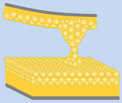
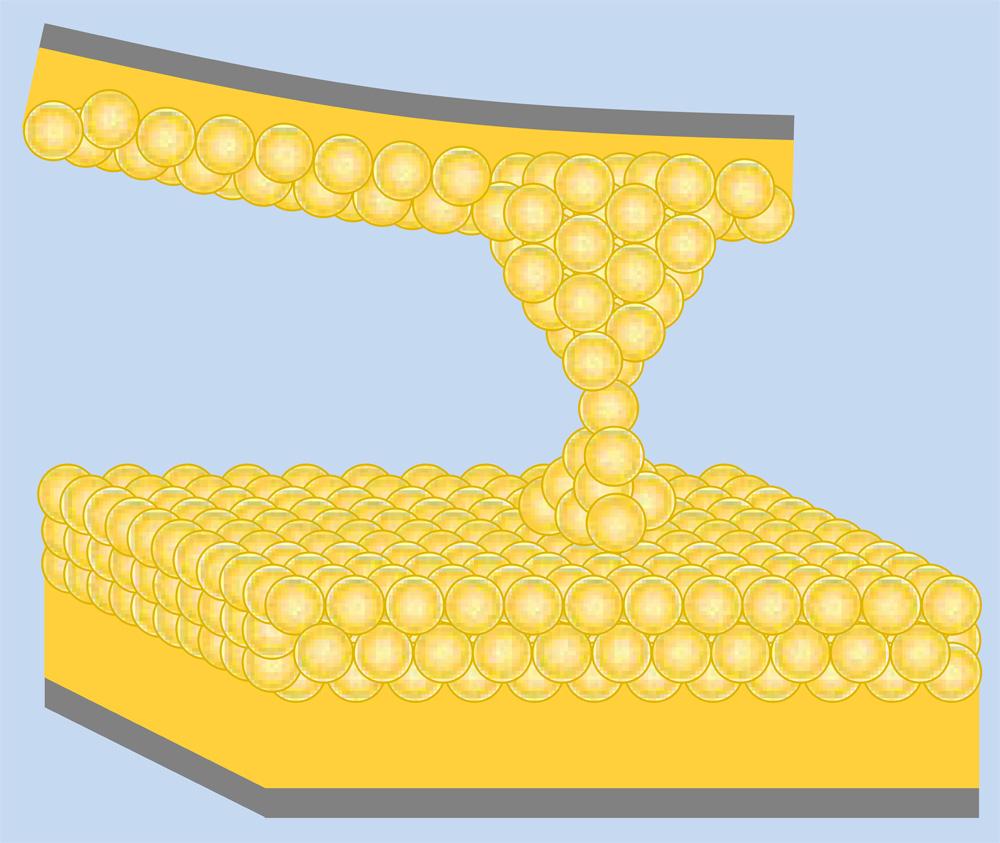
Harsh Deep Chopra and his colleagues at the State University of New York at Buffalo have been working on ways to probe physical parameters at the atomic scale. They looked at tiny gold contacts that develop where a sharp gold point, or “tip,” meets a flat gold surface. These connections, which can be as thin as one atom at their narrowest point, exhibit novel electrical and mechanical properties.
To estimate the number of atoms at the narrowest place, researchers typically apply a voltage and measure the electrical conductance. Previous experiments have shown sudden downward jumps in this conductance as the tip and surface were pulled apart, thinning the junction. These jumps were attributed to sudden atomic rearrangements [1]. Chopra’s team decided to probe the mechanics of these rearrangements as the number of atoms is varied from hundreds down to one. “Steadiness is key, since the goal is to push and pull on a single atom,” Chopra says.
The researchers applied stress to their gold contacts by advancing and retracting the surface toward and away from the tip in increments of 4 picometers. The tip was attached to a cantilever arm that measured the force and any change in the length of the contact. The ratio of force to length change gives the stiffness, or the related property called the Young’s modulus, which is a general measure of a material’s response to an applied pressure, independent of sample size.
As the contact gets narrower, a larger fraction of the atoms are on the surface, and their shorter, stiffer bonds–compared with those of internal atoms–should lead to a higher overall stiffness and higher modulus. Previous experiments have seen some evidence of this but were limited in the length scales studied. Chopra’s group observed a clear enhancement in the modulus below a width of one nanometer. In the limit of a single gold atom, the modulus grows to at least twice that of the normal, macroscopic gold modulus, the team found.
The team also investigated the process underlying the sudden jumps in conductance that previous work identified as abrupt atomic rearrangements. With their precision measurements, Chopra’s team was able to detect downward jumps in the length of the contact during compression. For example, when the narrowest point had fewer than 20 atoms, the length changed by one of four possible values: 49, 79, 88 or 98 picometers. The team found that these jumps correspond to the halting motion expected for gold atoms in a crystal that has cracked along an internal plane, where the two pieces slide past one another.
“The authors show that these re-arrangements are not random in nature (as one may expect), but rather always occur in units of crystallographic slip distances,” says Julia Greer of the California Institute of Technology in Pasadena. She thinks this will impact our understanding of how atomic-level physics influences large-scale mechanical properties. Jan van Ruitenbeek of Leiden University in the Netherlands agrees. He thinks the behavior of nanoscale contacts between metallic materials could give insight into friction and wear on these surfaces.
–Michael Schirber
Michael Schirber is a Corresponding Editor for Physics Magazine based in Lyon, France.
References
- G. Rubio, N. Agraït, and S. Vieira, “Atomic-Sized Metallic Contacts: Mechanical Properties and Electronic Transport,” Phys. Rev. Lett. 76, 2302 (1996)


