Atom Diffraction from a Microscopic Spot
Microscopy with atoms offers new possibilities in the study of surfaces and two-dimensional (2D) materials [1]. Atom beams satisfy the most important requirements for microscopic probing: they can achieve high contrast and surface-specificity while doing little damage to the sample. A subtype of atomic microscopy—atomic-diffraction imaging—obtains measurements in reciprocal, or momentum, space, which is ideal for studying the surfaces of large and uniform crystalline samples. However, scientists developing this technique face challenges in achieving micrometer-scale spatial resolutions that would allow the study of polycrystalline materials, nonuniform 2D materials, and other surfaces without long-range order. A team led by David Ward at the University of Cambridge, UK, has now used a collimated beam of helium atoms to measure a micrometer-sized spot on a crystal surface, generating image contrast via diffraction from the subatomic-scale corrugation of surface electrons [2]. Such selective imaging based on diffraction contrast opens new horizons in characterizing the composition and heterogeneity of 2D materials.
The advantages of atom beams as microscopic probes are largely due to the energy of the particles employed. For example, while conventional surface-imaging techniques rely on photons or electrons with energies ranging from electron volts to thousands of electron volts, in atomic microscopy the atoms have energies in the milli-electron-volt range. Unlike the “cannonballs” of high-energy particles, these atoms scatter like ping-pong balls, meaning they can be used to image a surface harmlessly and with excellent sensitivity.
Studies of atom–surface interactions stretch back to the early days of quantum mechanics when physicists Immanuel Estermann and Otto Stern first demonstrated diffraction of helium atoms at the surface of a crystal of lithium fluoride [3]. Soon after, resonances were discovered in the intensity of the scattered beam measured as a function of the energy of the incoming helium atoms. Such peaks were rapidly interpreted as indicating the presence of bound states of the projectile atoms on the surface: incoming helium atoms were temporarily trapped in potential wells above the crystal lattice. This observation opened up applications in the field of surface science, in particular by linking surface physics and surface chemistry through ubiquitous van der Waals forces. Atom diffraction was also instrumental in revealing the importance of surfaces for trapping reactants before catalytic reactions can occur.
Today, there are a variety of surface-characterization techniques based on the scattering of neutral atoms [4]. Diffraction measurements using either low-energy atoms or high-energy atoms at near grazing incidences provide extremely precise information about the subatomic structure of a surface. This information, however, is derived from measurements averaged over a relatively large area—typically a millimeter-sized spot—meaning that the material must exhibit long range on that scale. The actual spatial resolution of these techniques is therefore not sufficient to resolve microscopic domains in samples that aren’t perfect crystals [5].
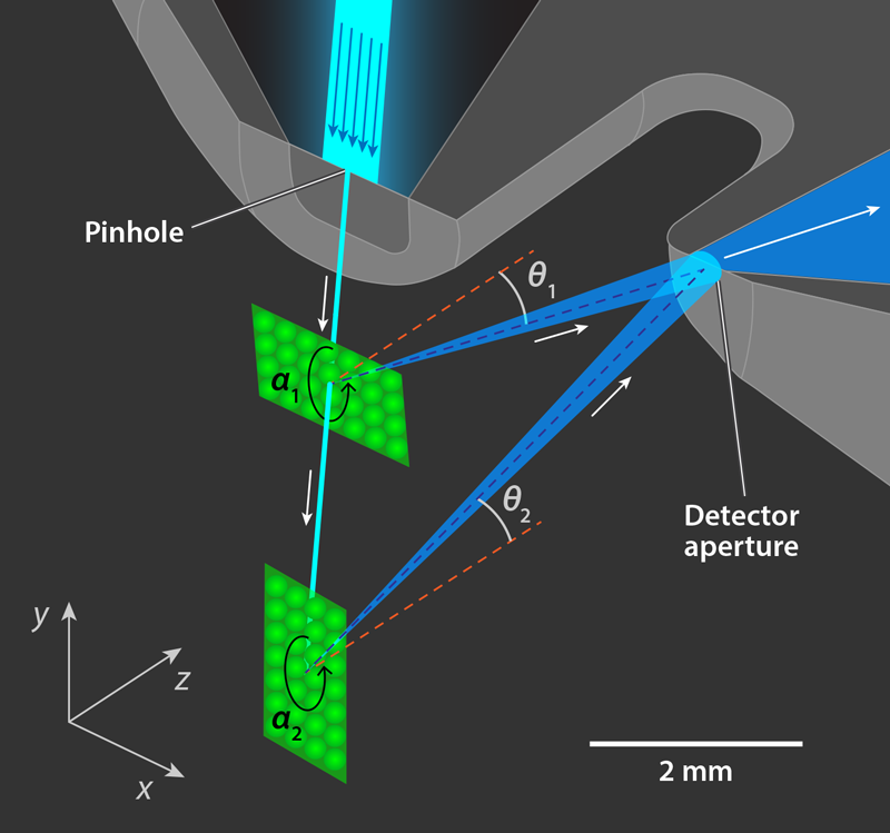
Ward and his colleagues overcome this resolution limit thanks to a collimated beam of helium atoms. They use accurate, computer-controlled piezoelectric actuators to maintain the position of this beam on a sample while varying the angle at which the scattered helium atoms are measured (Fig. 1). Probing a crystal of lithium fluoride, the researchers demonstrate the ability to record a diffraction pattern over a broad range of outgoing angles from a 10-micrometer-diameter spot. This micron-scale resolution is an improvement over existing atom-diffraction techniques by more than 2 orders of magnitude.
As well as outperforming previous atom-diffraction setups in terms of spatial resolution, the team also achieves excellent image contrast. The quality and information content of an image are defined by the contrast mechanism; an image with no contrast is essentially blank. In earlier atom-microscopy images, contrast was mainly obtained by measuring the direct effect of the topography on the scattered atoms, sometimes after first depositing heavy atoms on the sample’s surface to create artificial “shadows” [6]. In this sense, the new technique “emerges from the shadows”: by controlling the atom beam’s scattering angle, Ward and his colleagues generate image contrast by measuring the atom beam’s diffraction instead. These diffraction patterns deliver images with enhanced clarity and electronic specificity and provide new insights into the interaction potential between atom and surface.
The diffraction patterns also yield spatial accuracy between a tenth and a hundredth of the atom’s de Broglie wavelength, meaning the spatial modulation of the electron density in the surface of a sample can be measured with picometer precision. A similar precision can also be achieved using conventional atomic-diffraction techniques, but not over the small (micrometer-scale) areas that the researchers have now been able to probe. Being able to make such precise, spatially localized measurements will allow the investigation of mosaic domains—local differences in crystal alignment on nanometer scales—that are so important for materials science and for the rapidly growing field of thin-film technologies.
Despite the advance achieved by Ward and his colleagues, atom microscopy is still a new and emerging technique. While the principles are simple, the technical requirements are demanding. Limitations in the beam intensity and the detector sensitivity apply here, as in all microscopic techniques. As technology advances one may anticipate improvements in the rate at which images can be accumulated. Similarly, more sophisticated sample preparation methods and beams with variable energy [6] will allow greater control and flexibility in the acquisition of images. These developments would further enhance the reach of the technique and open up the study of a wider range of soft and delicate materials.
References
- A. S. Palau et al., “Neutral helium atom microscopy,” Ultramicroscopy 251, 113753 (2023).
- N. A. von Jeinsen et al., “2D helium atom diffraction from a microscopic spot,” Phys. Rev. Lett. 131, 236202 (2023).
- I. Estermann and O. Stern, “Beugung von Molekularstrahlen,” Z. Physik 61, 95 (1930).
- B. Holst et al., “Material properties particularly suited to be measured with helium scattering: selected examples from 2D materials, van der Waals heterostructures, glassy materials, catalytic substrates, topological insulators and superconducting radio frequency materials,” Phys. Chem. Chem. Phys. 23, 7653 (2021).
- M. Debiossac et al., “Refraction of fast Ne atoms in the attractive well of a LiF(001) surface,” J. Phys. Chem. Lett. 11, 4564 (2020).
- M. Barr et al., “Unlocking new contrast in a scanning helium microscope,” Nat. Commun. 7, 10189 (2016).