A Bird’s Eye View of Circuit Photons
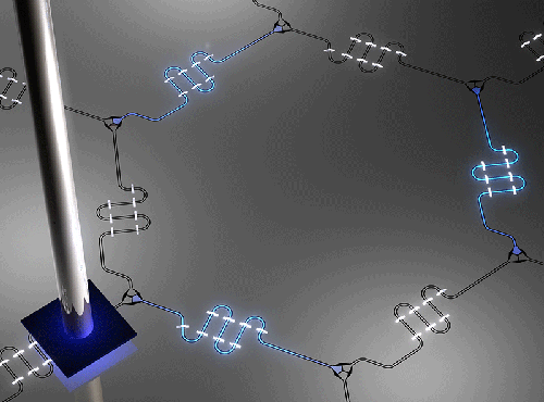
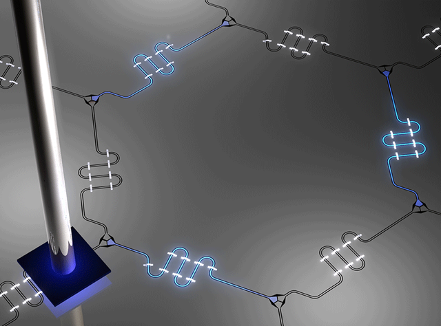
Quantum mechanics rules the dynamics of light and matter. Yet performing a quantum-mechanical simulation of a material from first principles is practically impossible on a classical computer because the complexity of the simulation increases exponentially with the number of particles involved. The solution, according to Richard Feynman, was to build a machine out of quantum building blocks that could directly emulate the material itself [1]. Prototypes of such quantum simulators that are based on ultracold atoms, ions, photons, and superconducting microwave circuits are now available [2], with the latter, in particular, having attracted Silicon Valley’s interest. The challenge with these circuit-based simulators, however, is that they are 2D, which complicates the readout of their constituent elements. Andrew Houck from Princeton University, New Jersey, and colleagues have now delivered an attractive solution by developing a technique [3], called scanning defect microscopy (Fig. 1), that determines the number of photons occupying each mode of a 2D microwave circuit. It is this information that would serve as the fundamental input and output for certain quantum simulations.
Superconducting microwave circuits combine electronic and photonic degrees of freedom [4, 5]. The main element of the circuit is a transmission line, which is made up of a central superconducting wire separated by a gap from two grounded plates. All of these structures are on a single plane, as if one had taken a 2D slice through a coaxial cable. When truncated, the transmission line becomes a resonator, which can host discrete photon modes within its gaps. Large lattices of resonators can be engineered in various 1D or 2D geometries by coupling two, three, or more resonators together via a capacitive interface. In many ways, photons in such devices behave similarly to electrons in a solid.
To make microwave circuits that can simulate quantum phenomena faster than a classical computer, however, resonator lattices have to be integrated with superconducting qubits. Such qubits are controlled with electrical currents in a Josephson tunnel junction, and in many respects, they behave like artificial atoms, which couple to the photons in the circuit. As a result, superconducting microwave circuits can be used to explore the coupling between the quantum states of light and matter, the regime of circuit quantum electrodynamics (cQED). Photons in these devices often exhibit striking matter-like behavior [6, 7], providing the basis for the simulation of complex materials. Such circuits can be fabricated on a substrate using standard lithographic techniques, with qubits and resonators that are hundreds of micrometers or even millimeters in size.
Small-scale realizations of cQED lattices have already been used for proof-of-principle quantum simulations [8, 9]. However, future large-scale simulations will have to be initialized and measured efficiently—steps known as drive and readout. This requires connecting the lattices to external circuitry, such as voltage sources, circulators, and amplifiers, which typically reside outside the chip. So far, this connectivity has been realized through external transmission lines, but these elements can only couple to the resonators at the edges of the lattice because of its 2D nature. Such a side view provides only limited information about the quantum state and spatial correlations of photons inside the bulk resonators, seriously limiting the applicability of circuit QED devices for quantum simulations.
The probe developed by Houck and colleagues, scanning defect microscopy (SDM), solves this problem by moving outside the plane of the chip to provide a fuller image of photons within the chip. In SDM, a small sapphire tip is positioned a few tens of micrometers above the surface of one of the resonators (Fig. 1). The presence of this dielectric modifies the evanescent electric field from the circuit photons, which extends just outside the plane of the chip. Specifically, the tip increases the local capacitance of the transmission line, downshifting the local resonator frequency. This in turn causes a drop in the transmission of photons through the lattice when it is driven at its nominal resonance frequency.
Houck’s team showed that if the sapphire tip has only a weak (linear) effect on the resonator frequency, then a simple analytic relationship exists between the induced frequency shift, the change in transmission, and the local photonic occupation of each resonator. This relationship provides a recipe for detecting the local photon occupancy inside the lattice. First, calibrate the probe by determining the frequency shift for a single isolated resonator as a function of the tip’s position. Second, measure the transmission through the whole lattice with and without the probe. Finally, use the measured transmission drop with the probe present to find the photonic occupation of an individual resonator in the lattice. A map of the photon-mode occupancies can be obtained by scanning the probe across the whole lattice.
Houck’s team used SDM to image the occupancies of the photon modes of 49 coupled resonators arranged in a special geometry called a kagome lattice (see details in Fig. 1). (To simplify the measurement, no superconducting qubits were incorporated with the resonators.) The occupancies they measured were in excellent agreement with theoretical predictions, corresponding to a fidelity of 0.99. The high fidelity is even more impressive considering the weak signal-to-noise ratio of their technique (which is limited by the intentionally small size of the frequency-shifted region) and the technical challenge of positioning the probe inside a cryostat for in situ measurements.
While SDM shares similarities with so-called bead-pull experiments for accelerators and scanning gate microscopy for nanostructures, it is truly a new tool for quantum electronics. The first application of SDM is likely to be the simulation of 2D topological phenomena and geometrically frustrated lattices (of which the kagome lattice is one example.) Both are associated with macroscopically degenerate systems, which are notoriously difficult to simulate on a classical computer. Such circuits are genuinely open systems (photons can be added or lost). This, combined with their inherent strong light-matter coupling, makes such quantum simulators ideal candidates for the study of many-body, out-of-equilibrium phenomena, such as thermalization or nonequilibrium phase transitions. SDM could also lead to the discovery of new exotic phenomena, which are unknown in traditional solid-state systems. In a nutshell, SDM constitutes a new and indispensible tool for future experiments on quantum simulations with microwave photons.
This research is published in Physical Review X.
References
- R. Feynman, “Simulating Physics with Computers,” Int. J. Theor. Phys. 21, 467 (1982).
- I. M. Georgescu, S. Ashhab, and Franco Nori, “Quantum Simulation,” Rev. Mod. Phys. 86, 153 (2014).
- D. L. Underwood, W .E. Shanks, A. C. Y. Li, L. Ateshian, J. Koch, and A. A. Houck, “Imaging Photon Lattice States by Scanning Defect Microscopy,” Phys. Rev. X 6, 021044 (2016).
- A. Blais, R.-S. Huang, A. Wallraff, S. M. Girvin, and R. J. Schoelkopf, “Cavity Quantum Electrodynamics for Superconducting Electrical Circuits: An Architecture for Quantum Computation,” Phys. Rev. A 69, 062320 (2004).
- A. Wallraff, D. I. Schuster, A. Blais, L. Frunzio, R.- S. Huang, J. Majer, S. Kumar, S. M. Girvin, and R. J. Schoelkopf, “Strong Coupling of a Single Photon to a Superconducting Qubit Using Circuit Quantum Electrodynamics,” Nature 431, 162 (2004).
- A. A. Houck, H. E. Türeci, and J. Koch, “On-Chip Quantum Simulation with Superconducting Circuits,” Nature Phys. 8, 292 (2012).
- S. Schmidt and J. Koch, “Circuit QED Lattices: Towards Quantum Simulation with Superconducting Circuits,” Ann. Phys. 525, 395 (2013).
- D. L. Underwood, W. E. Shanks, Jens Koch, and A. A. Houck, “Low-Disorder Microwave Cavity Lattices for Quantum Simulation with Photons,” Phys. Rev. A 86, 1 (2012).
- J. Raftery, D. Sadri, S. Schmidt, H. E. Türeci, and A. A. Houck, “Observation of a Dissipation-Induced Classical to Quantum Transition,” Phys. Rev. X 4, 031043 (2014).


