Waves on a Plane
Light can mix with electrons to form a wave that travels along a metal surface and which might enable high-speed, “plasmonic” devices. In the 15 February Physical Review Letters, researchers show theoretically how to solve one of the practical problems with these waves–they lose energy whenever they encounter something other than a plain surface, like the equivalent of a mirror or lens. The team’s calculations show how to eliminate the energy loss using materials engineered with unusual electrical properties. Such improvements could allow researchers to make devices on chips that mimic those used with ordinary light waves.
Light signals are the 18-wheelers of the internet, cheaply hauling large loads of data over long distances. But like the interstates the big rigs ply, waveguides that channel photons of light must curve gently to keep the cargo on course. As a result, structures for manipulating light tend to be big–much larger than the micron-scale wavelength of light. One way to confine light more tightly is to shine it onto a metal surface. When conditions are right, the light combines with a “plasmon”–a sloshing motion of the electrons–to form a new mode that travels only along the surface and that turns corners like a sports car.
Placing an additional insulating layer of material on top of the metal alters the speed of this combined wave, which is called a surface plasmon polariton or SPP. Researchers can exploit this speed variation by putting different materials in different regions to control the two-dimensional waves, just as a properly shaped lens uses the varying speed of light in glass to manipulate ordinary light. Researchers dream of an SPP optics-table-on-a-chip, where lenses, filters, and mirrors could process light signals more efficiently than the electronic circuits that handle today’s fiber-optic communications.
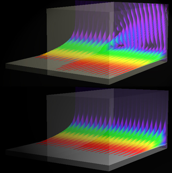
Unfortunately, says Viktor Podolskiy of Oregon State University in Corvallis, when SPPs hit the border between regions with different speeds, as much as 30% of their energy scatters away into the third dimension. This scattering occurs because, in regions where the wave travels slower, its energy is also more tightly confined to the metal surface than in faster regions. The mismatch in confinement prevents the wave from efficiently crossing a border and makes complex structures impractical.
Podolskiy and graduate student Justin Elser propose covering the metal with materials whose electrical properties vary strongly with direction. If the material’s response to an electric field in the direction perpendicular to the metal is very different from its response in the parallel direction, it turns out that the degree of confinement can be adjusted and matched across a border. “The anisotropy buys you independent control of the mode structure” and the speed, Podolskiy says. In their paper, the researchers show that such a material practically eliminates the unwanted scattering for two specific examples of optics devices–a simple filter and an SPP “magnifying superlens,” a structure made of concentric rings of different materials.
The required anisotropic material could be a so-called metamaterial, Podolskiy says, one with nanoscale structures engineered for specific responses to electric and magnetic fields. In addition, he says, researchers might achieve the same effect using materials whose optical properties change in a static electric field, which could open the door to electrically reconfigurable plasmonic devices.
Harry Atwater of the California Institute of Technology in Pasadena says that “out-of-plane scattering is not as big an issue as metal absorption” in sapping the energy of SPPs. But he notes that exploiting anisotropic materials could be a useful tool in plasmonics, as well as in other optical systems.
–Don Monroe
Don Monroe is a freelance science writer in Murray Hill, New Jersey.
More Information
Focus story on focusing of surface waves from 2003