All-Mechanical Control of Single Electrons
The ability to manipulate individual electrons with atomic precision is essential to the development of nanometer-scale electronics. In previous studies, researchers were able to control the charge state of single atoms on a surface using scanning-tunneling or atomic force microscopes. However, these studies could not combine high spatial resolution with the stable positioning of charges. A research team led by Robert Wolkow at the University of Alberta in Canada has now demonstrated that they can place and detect a single electron with atomic resolution using an all-mechanical approach.
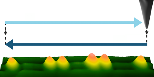
The scheme uses an atomic force microscope (AFM) to control the charge state of dangling bonds (DBs) on a silicon surface. Owing to their unfilled valence, each DB can localize an electron and act as charge host. As the researchers lowered the AFM tip closer to the surface, they observed that the DB just under the tip underwent a sudden transition from neutral to negatively charged. This effect is rooted in the attractive force between the tip and surface, which lifts a silicon atom, causing it to rehybridize in a way that favors the negatively charged state. The researchers used this effect to “write” charge onto a bond; they could then also “read” the charge state with the same tip by moving the tip further away from the surface. In contrast to previous studies with similar setups, the effect is purely mechanical and doesn’t require a bias voltage. This voltage would cause, through quantum tunneling, a current that would prevent the stable trapping of the charge.
The new experiments also showed that the charge-writing process is reproducible and reversible and yields a charge configuration that is stable for many seconds. The team applied this protocol to structures containing up to six DBs, showing that the approach could be scaled up to realize more complex nanocircuits.
This research is published in Physical Review Letters.
–Nicolas Doiron-Leyraud
Nicolas Doiron-Leyraud is a Corresponding Editor for Physics and a researcher at the University of Sherbrooke.
Correction (05 November 2018): The text was modified to explicitly define the “write” and “read” steps.