Enhanced Emission for Improved Electron Spectroscopy
When the electron microscope was invented in 1931, scientists could, for the first time, image objects much smaller than optical microscopes would allow. The invention laid the foundation for atomic- and molecular-scale imaging of the natural and engineered world. Nowadays, subatomic spatial resolution is possible, and scientists are also adding “color”—spectroscopic information—to their images, revealing materials’ chemical compositions as well as their electronic, phononic, magnetic, and optical properties. Such spectral information is key to understanding the function of catalysts, batteries, quantum materials, and biological systems [1–3], to name a few. The technique is still nascent, however, offering only limited energy resolution. To further improve the capabilities of electron spectroscopy, Alexander Stibor from the Lawrence Berkeley National Laboratory, California, and the University of Tübingen, Germany, along with his colleagues have developed a bright, highly collimated electron source with a narrow spectral width, promising record energy resolution [4]. This new technology could lead to high-resolution imaging in previously unmeasured “colors” that can also reveal molecular vibrational modes.
Conventional methods for measuring molecular vibrations, phonon modes, and other interesting material properties are generally based on optical processes—direct optical absorption (for example, Fourier-transform infrared spectroscopy) or incident light energy changes (for example, Raman spectroscopy)—yet these optical methods are limited by the diffraction limit of light. In electron microscopes, electron energy-loss spectroscopy can measure changes in electron energy as electrons pass through the material and excite various material transitions, including vibrations [1]. Importantly, the method can achieve a spatial resolution comparable to the size of the electron beam. Yet high spectral resolution is challenging, as molecular vibrations occur at energies in the meV range whereas electron beams typically operate at around 300 keV. Overcoming the ten-order-of-magnitude difference in energy is akin to measuring the speed of a jogger while traveling at light speed. To achieve meV energy resolution with a keV beam requires incredible control of the electron source.
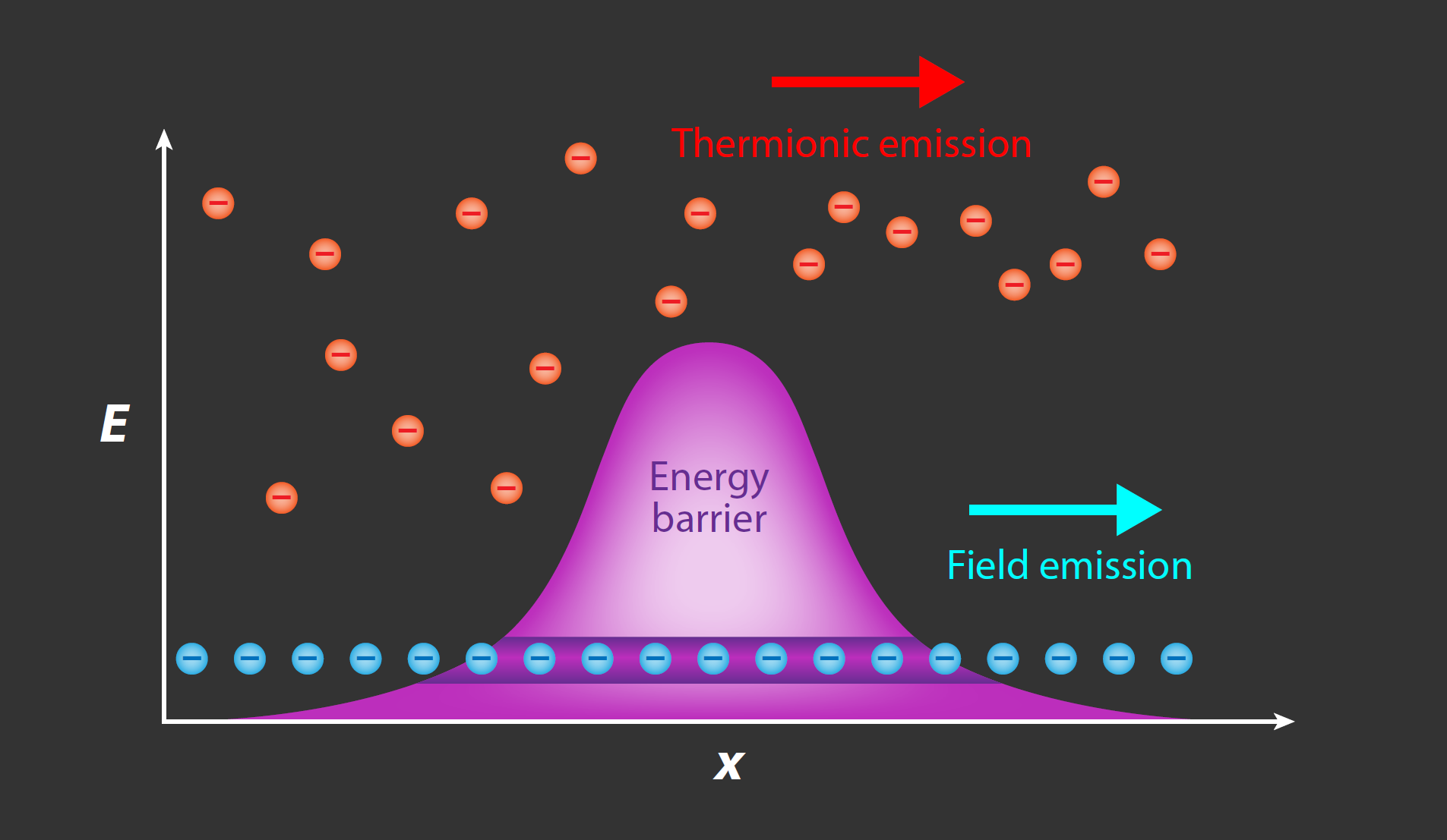
Such sources can be described by three key parameters: their brightness (how many electrons are emitted per second), their coherence (the similarity in phase and energy of each emitted electron, which determines the spatial and energy resolution), and their stability. Sources emit electrons via two major mechanisms: thermionic emission and field emission (Fig. 1). In thermionic emission, the work function of a metal’s conduction electrons is overcome either by heating a high-melting-point metal to a very high temperature or by heating a low-work-function metal to a less extreme temperature. However, electron guns that operate using thermionic emission suffer from low brightness and broad electron-energy spreads of a few eV, resulting in limited temporal and spatial coherence.
Devices based on field emission are a newer alternative to thermionic emitters and offer improvements in both brightness and energy spread. In field-emission guns (FEGs), localized emission occurs at a sharp tip, where significant electron field enhancement allows electrons at the Fermi level to tunnel directly through the potential energy barrier under an applied electrostatic field [5]. The most common field emitter is a tungsten “hairpin” filament with a sharp tip (apex radius of ∼100 nm); this filament is used as a steady-state electron source in most cold FEG electron microscopes. Recent research into electron sources has suggested a variety of alternative materials for FEGs, such as single-crystal copper [6], graphene [7], and carbon nanotubes [8], which have all demonstrated breakthroughs in emitter energy resolution and brightness. However, these emitters often come with trade-offs between different performance metrics.
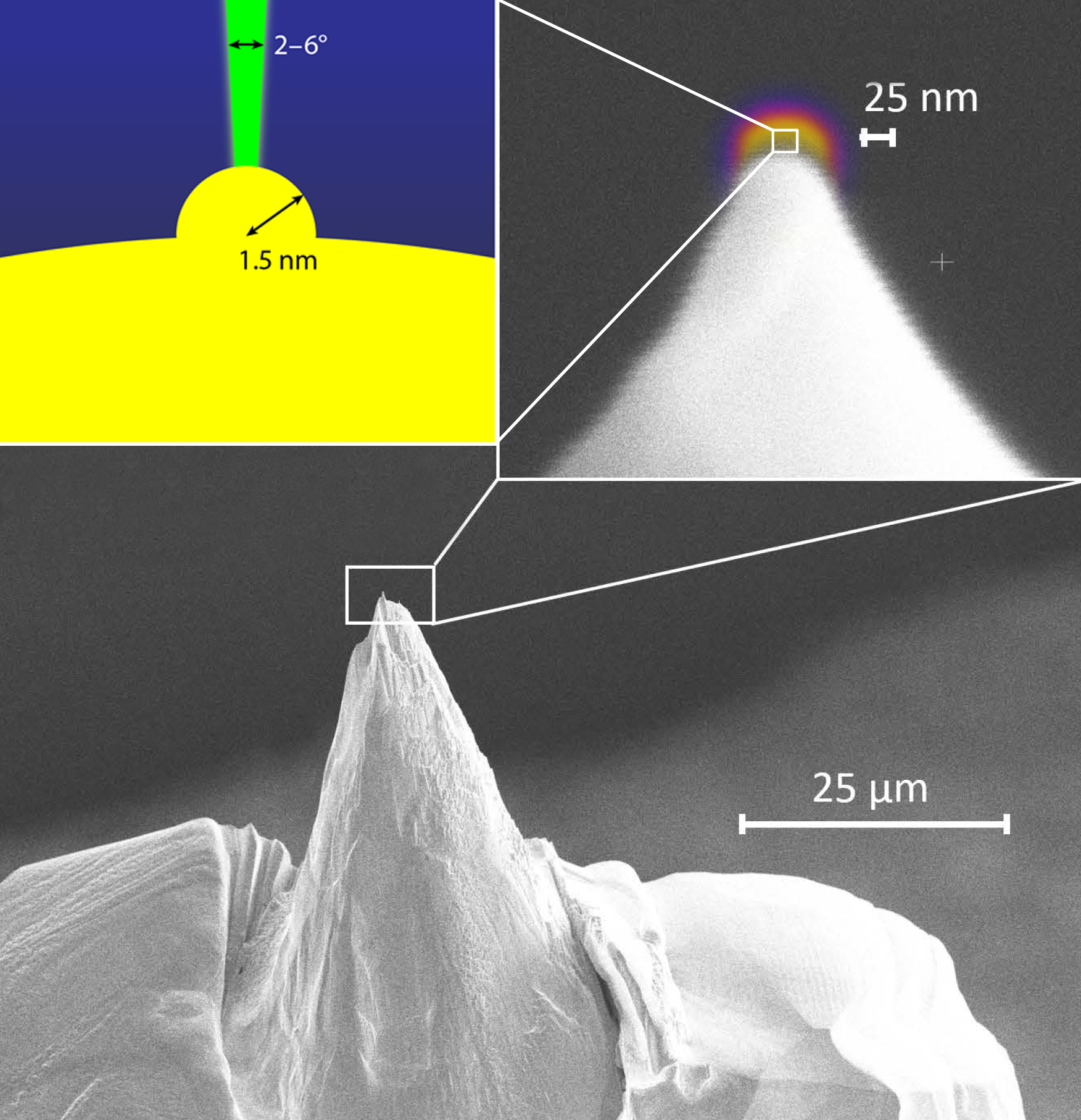
Stibor and his colleagues have developed a steady-state FEG that requires no such trade-offs, offering optimal performance in brightness, coherence, and stability. They fabricate a monocrystalline niobium (Nb) “nanotip” with a radius of curvature of around 25 nm that has an even smaller “nanoprotrusion” (radius of curvature of 1.5 nm) at its apex (Fig. 2). They cool this extremely sharp tip to 5.9 K (below Nb’s relatively high critical temperature for superconductivity of 9.35 K) and apply a varying electric field to extract electrons from its end. The nanoprotrusion’s small size means that it supports localized modes, while its sharp radius of curvature highly enhances the electric field at the apex, allowing electrons to tunnel into the separate modes. The result is that, unlike in conventional FEGs, the electrons are emitted at discrete, resonant energies. Importantly, these energies are linearly tunable with the applied electric field at the tip [9].
By tuning this electric field, the researchers were able to shift the electron energy distribution until a resonance appeared near the Fermi energy. Additionally, at the low temperature used in their experiment, few electrons have enough thermal energy to occupy states above the Fermi energy, which therefore acts as a sharp cutoff [10]. As the tuned energy distribution approaches this Fermi-edge upper bound, the electrons are restricted to a narrow energy range, down to a width of 16 meV—an energy spread an order-of-magnitude smaller than that of the best tungsten electron field emitter. Combined with a standard monochromator—a commonly used component that can improve the energy resolution even further (as low as 2.5 meV)—this result translates into an order-of-magnitude improvement in the spectral resolution of state-of-the-art electron spectroscopies [1].
Stibor and colleagues additionally demonstrate their emitter’s reproducibility, stability, and brightness. Because of the self-focusing nature of the nanoprotrusion, the electron beam is emitted at ultranarrow emission angles (2–6°), leading to increased electron spatial density. The team’s device also avoids having to trade this high brightness for energy resolution as conventional electron microscopes do. For instance, in a conventional device, a monochromator narrows the energy width by removing electrons outside of a certain energy range, thereby decreasing the brightness proportionally. The Nb nanotip, on the other hand, can exhibit a high brightness (two-orders-of-magnitude higher than a commercial FEG with an active monochromator) while maintaining an ultranarrow energy resolution and a tunable energy distribution.
This breakthrough will open new avenues for vibrational spectroscopy using electron microscopes. For example, the single-digit-meV resolution will enable detection, differentiation, and quantification of various chemical species, including atomic isotopes [11] and molecular isomers. The high coherence of the emitter can also enable quantum electron microscopy [12], where interactions between the electron beam and the imaged sample are minimized without losing information. This technique could revolutionize imaging of electron-beam-sensitive samples, such as biological specimens and various weakly scattering quantum materials. Finally, there could also be applications beyond electron microscopy, including emission of entangled electron pairs for quantum information sciences and quantum metrology. Though one can only speculate on the many opportunities that will be enabled by this “sharp” invention, one thing is certain: electron microscopy has, in the words of an old candy commercial, “tasted the rainbow.”
References
- O. L. Krivanek et al., “Vibrational spectroscopy in the electron microscope,” Nature 514, 209 (2014).
- D. F. Swearer et al., “Advancing plasmon-induced selectivity in chemical transformations with optically coupled transmission electron microscopy,” Acc. Chem. Res. 54, 3632 (2021).
- N. M. Pirozzi et al., “ColorEM: Analytical electron microscopy for element-guided identification and imaging of the building blocks of life,” Histochem. Cell Biol. 150, 509 (2018).
- C. W. Johnson et al., “Near-monochromatic tuneable cryogenic niobium electron field emitter,” Phys. Rev. Lett. 129, 244802 (2022).
- L. E. Franken et al., “Transmission electron microscopy as a tool for the characterization of soft materials: Application and interpretation,” Adv. Sci. 4, 1600476 (2017).
- S. Karkare et al., “Ultracold electrons via near-threshold photoemission from single-crystal Cu(100),” Phys. Rev. Lett. 125, 054801 (2020).
- X. Shao et al., “A high-brightness large-diameter graphene coated point cathode field emission electron source,” Nat. Commun. 9, 1288 (2018).
- F. Giubileo et al., “Field emission from carbon nanostructures,” Appl. Sci. 8, 526 (2018).
- V. T. Binh et al., “Field-emission electron spectroscopy of single-atom tips,” Phys. Rev. Lett. 69, 2527 (1992).
- Haonan Huang et al., “Tunnelling dynamics between superconducting bound states at the atomic limit,” Nat. Phys. 16, 1227 (2020).
- J. A. Hachtel et al., “Isotope-resolved electron energy loss spectroscopy in a monochromated scanning transmission electron microscope,” Micros. Today 29, 36 (2021).
- P. Kruit et al., “Designs for a quantum electron microscope,” Ultramicroscopy 164, 31 (2016).


